 | –≠–ª–µ–∫—Ç—Ä–æ–Ω–Ω—ã–π –∫–æ–º–ø–æ–Ω–µ–Ω—Ç: 74HC1GU04 | –°–∫–∞—á–∞—Ç—å:  PDF PDF  ZIP ZIP |

DATA SHEET
Product specification
File under Integrated Circuits, IC06
1998 Nov 18
INTEGRATED CIRCUITS
74HC1GU04
Inverter
1998 Nov 18
2
Philips Semiconductors
Product specification
Inverter
74HC1GU04
FEATURES
∑
Wide operating voltage:
2.0 to 6.0 V
∑
Symmetrical output impedance
∑
Low power dissipation
∑
Balanced propagation delays
∑
Very small 5-pin package
∑
Output capability: standard.
DESCRIPTION
The 74HC1GU04 is a high-speed
Si-gate CMOS device.
The 74HC1GU04 provides the
inverting single stage function.
The standard output currents are
1
/
2
compared to the 74HCU04.
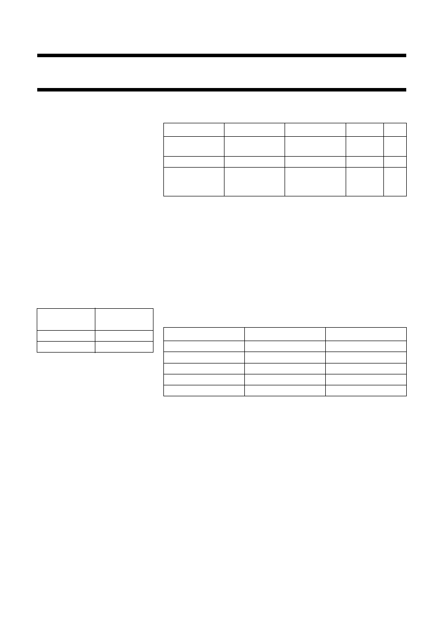
FUNCTION TABLE
See note 1.
Note
1. H = HIGH voltage level;
L = LOW voltage level.
INPUT
inA
OUTPUT
outY
L
H
H
L
QUICK REFERENCE DATA
GND = 0 V; T
amb
= 25
∞
C; t
r
= t
f
= 6.0 ns.
Notes
1. C
PD
is used to determine the dynamic power dissipation (P
D
in
µ
W).
P
D
= C
PD
◊
V
CC
2
◊
f
i
+
(C
L
◊
V
CC
2
◊
f
o
) where:
f
i
= input frequency in MHz;
f
o
= output frequency in MHz;
C
L
= output load capacitance in pF;
V
CC
= supply voltage in V;
(C
L
◊
V
CC
2
◊
f
o
) = sum of outputs.
2. For HC1G the condition is V
I
= GND to V
CC.
PINNING
SYMBOL
PARAMETER
CONDITIONS
TYP.
UNIT
t
PHL
/t
PLH
propagation
delay inA to outY
C
L
= 15 pF;
V
CC
= 5 V
5
ns
C
I
input capacitance
5
pF
C
PD
power
dissipation
capacitance
notes 1 and 2
14
pF
PIN
SYMBOL
DESCRIPTION
1
n.c.
not connected
2
inA
data input
3
GND
ground (0 V)
4
outY
data output
5
V
CC
DC supply voltage

1998 Nov 18
3
Philips Semiconductors
Product specification
Inverter
74HC1GU04
ORDERING INFORMATION
OUTSIDE NORTH
AMERICA
PACKAGES
TEMPERATURE
RANGE
PINS
PACKAGE
MATERIAL
CODE
MARKING
74HC1GU04GW
-
40 to +125
∞
C
5
SC-88A
plastic
SOT353
HD
Fig.1 Pin configuration.
handbook, halfpage
1
2
3
5
4
MNA042
U04
VCC
inA
outY
GND
n.c.
Fig.2 Logic symbol.
handbook, halfpage
MNA043
inA
outY
2
4
Fig.3 IEC logic symbol.
handbook, halfpage
2
1
4
MNA044
Fig.4 Logic diagram.
handbook, halfpage
MNA045
inA
outY
1998 Nov 18
4
Philips Semiconductors
Product specification
Inverter
74HC1GU04
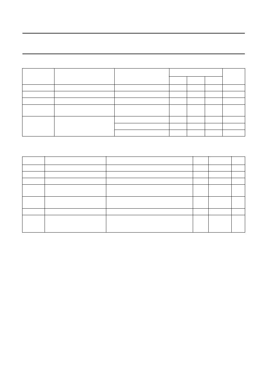
RECOMMENDED OPERATING CONDITIONS
LIMITING VALUES
In accordance with the Absolute Maximum Rating System (IEC 134). Voltages are referenced to GND (ground = 0 V).
Note
1. The input and output voltage ratings may be exceeded if the input and output current ratings are observed.
SYMBOL
PARAMETER
CONDITIONS
74HC1G
UNIT
MIN.
TYP.
MAX.
V
CC
DC supply voltage
2.0
5.0
6.0
V
V
I
input voltage
0
-
V
CC
V
V
O
output voltage
0
-
V
CC
V
T
amb
operating ambient
temperature range
see DC and AC
characteristics per device
-
40
+25
+125
∞
C
t
r
, t
f
input rise and fall times except
for Schmitt-trigger inputs
V
CC
= 2.0 V
-
-
1000
ns
V
CC
= 4.5 V
-
-
500
ns
V
CC
= 6.0 V
-
-
400
ns
SYMBOL
PARAMETER
CONDITIONS
MIN.
MAX.
UNIT
V
CC
DC supply voltage
-
0.5
+7.0
V
±
I
IK
DC input diode current
(1)
V
I
< -
0.5 or V
I
>
V
CC
+ 0.5 V
-
20
mA
±
I
OK
DC output diode current
(1)
V
O
< -
0.5 or V
O
>
V
CC
+ 0.5 V
-
20
mA
±
I
O
DC output source or sink
current standard outputs
(1)
-
0.5 V
<
V
O
<
V
CC
+ 0.5 V
-
12.5
mA
±
I
CC
DC V
CC
or GND current for
types with standard outputs
(1)
-
25
mA
T
stg
storage temperature range
-
65
+150
∞
C
P
D
power dissipation per
package 5 pins plastic SC-88A
for temperature range:
-
40 to +125
∞
C;
above +55
∞
C P
D
derates linearly with
2.5 mW/K
-
200
mW
1998 Nov 18
5
Philips Semiconductors
Product specification
Inverter
74HC1GU04
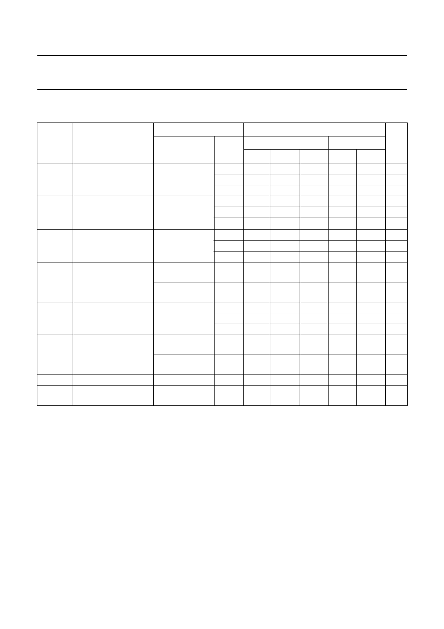
DC CHARACTERISTICS FOR THE 74HC1GU04
Over recommended operating conditions. Voltage are referenced to GND (ground = 0 V).
Note
1. All typical values are measured at T
amb
= 25
∞
C.
SYMBOL
PARAMETER
TEST CONDITIONS
T
amb
(
∞
C)
UNIT
OTHER
V
CC
(V)
-
40 to +85
-
40 to +125
MIN.
TYP.
(1)
MAX.
MIN.
MAX.
V
IH
HIGH-level input
voltage
2.0
1.7
1.4
-
1.7
-
V
4.5
3.6
2.6
-
3.6
-
V
6.0
4.8
3.4
-
4.8
-
V
V
IL
LOW-level input voltage
2.0
-
0.6
0.3
-
0.3
V
4.5
-
1.9
0.9
-
0.9
V
6.0
-
2.6
1.2
-
1.2
V
V
OH
HIGH-level output
voltage; all outputs
V
I
= V
IH
or V
IL
,
-
I
O
= 20
µ
A
2.0
1.8
2.0
-
1.8
-
V
4.5
4.0
4.5
-
4.0
-
V
6.0
5.5
6.0
-
5.5
-
V
V
OH
HIGH-level output
voltage; standard
outputs
V
I
= V
IH
or V
IL
,
-
I
O
= 2.0 mA
4.5
4.13
4.32
-
3.7
-
V
V
I
= V
IH
or V
IL
,
-
I
O
= 2.6 mA
6.0
5.63
5.81
-
5.2
-
V
V
OL
LOW-level output
voltage; all outputs
V
I
= V
IH
or V
IL
,
I
O
= 20
µ
A
2.0
-
0
0.2
-
0.2
V
4.5
-
0
0.5
-
0.5
V
6.0
-
0
0.5
-
0.5
V
V
OL
LOW-level output
voltage; standard
outputs
V
I
= V
IH
or V
IL
,
I
O
= 2.0 mA
4.5
-
0.15
0.33
-
0.4
V
V
I
= V
IH
or V
IL
,
I
O
= 2.6 mA
6.0
-
0.16
0.33
-
0.4
V
I
I
input leakage current
V
I
= V
CC
or GND
6.0
-
-
1.0
-
1.0
µ
A
I
CC
quiescent supply
current
V
I
= V
CC
or GND,
I
O
= 0
6.0
-
-
10
-
20
µ
A