 | –≠–ª–µ–∫—Ç—Ä–æ–Ω–Ω—ã–π –∫–æ–º–ø–æ–Ω–µ–Ω—Ç: 74HC273D | –°–∫–∞—á–∞—Ç—å:  PDF PDF  ZIP ZIP |

DATA SHEET
Product specification
File under Integrated Circuits, IC06
September 1993
INTEGRATED CIRCUITS
74HC/HCT273
Octal D-type flip-flop with reset;
positive-edge trigger
For a complete data sheet, please also download:
∑
The IC06 74HC/HCT/HCU/HCMOS Logic Family Specifications
∑
The IC06 74HC/HCT/HCU/HCMOS Logic Package Information
∑
The IC06 74HC/HCT/HCU/HCMOS Logic Package Outlines
September 1993
2
Philips Semiconductors
Product specification
Octal D-type flip-flop with reset;
positive-edge trigger
74HC/HCT273
FEATURES
∑
Ideal buffer for MOS microprocessor or memory
∑
Common clock and master reset
∑
Eight positive edge-triggered D-type flip-flops
∑
See "377" for clock enable version
∑
See "373" for transparent latch version
∑
See "374" for 3-state version
∑
Output capability; standard
∑
I
CC
category: MSI
GENERAL DESCRIPTION
The 74HC/HCT273 are high-speed Si-gate CMOS devices
and are pin compatible with low power Schottky TTL
(LSTTL). They are specified in compliance with JEDEC
standard no. 7A.
The 74HC/HCT273 have eight edge-triggered, D-type
flip-flops with individual D inputs and Q outputs. The
common clock (CP) and master reset (MR) inputs load and
reset (clear) all flip-flops simultaneously.
The state of each D input, one set-up time before the
LOW-to-HIGH clock transition, is transferred to the
corresponding output (Q
n
) of the flip-flop.
All outputs will be forced LOW independently of clock or
data inputs by a LOW voltage level on the MR input.
The device is useful for applications where the true output
only is required and the clock and master reset are
common to all storage elements.
QUICK REFERENCE DATA
GND = 0 V; T
amb
= 25
∞
C; t
r
= t
f
= 6 ns
Notes
1. C
PD
is used to determine the dynamic power dissipation (P
D
in
µ
W):
P
D
= C
PD
◊
V
CC
2
◊
f
i
+
(C
L
◊
V
CC
2
◊
f
o
) where:
f
i
= input frequency in MHz
f
o
= output frequency in MHz
(C
L
◊
V
CC
2
◊
f
o
) = sum of outputs
C
L
= output load capacitance in pF
V
CC
= supply voltage in V
2. For HC the condition is V
I
= GND to V
CC
For HCT the condition is V
I
= GND to V
CC
-
1.5 V
ORDERING INFORMATION
See
"74HC/HCT/HCU/HCMOS Logic Package Information"
.
SYMBOL
PARAMETER
CONDITIONS
TYPICAL
UNIT
HC
HCT
t
PHL/
t
PLH
propagation delay
C
L
= 15 pF; V
CC
= 5 V
CP to Q
n
15
15
ns
MR to Q
n
15
20
ns
f
max
maximum clock frequency
66
36
MHz
C
I
input capacitance
3.5
3.5
pF
C
PD
power dissipation capacitance per flip-flop
notes 1 and 2
20
23
pF
September 1993
3
Philips Semiconductors
Product specification
Octal D-type flip-flop with reset;
positive-edge trigger
74HC/HCT273
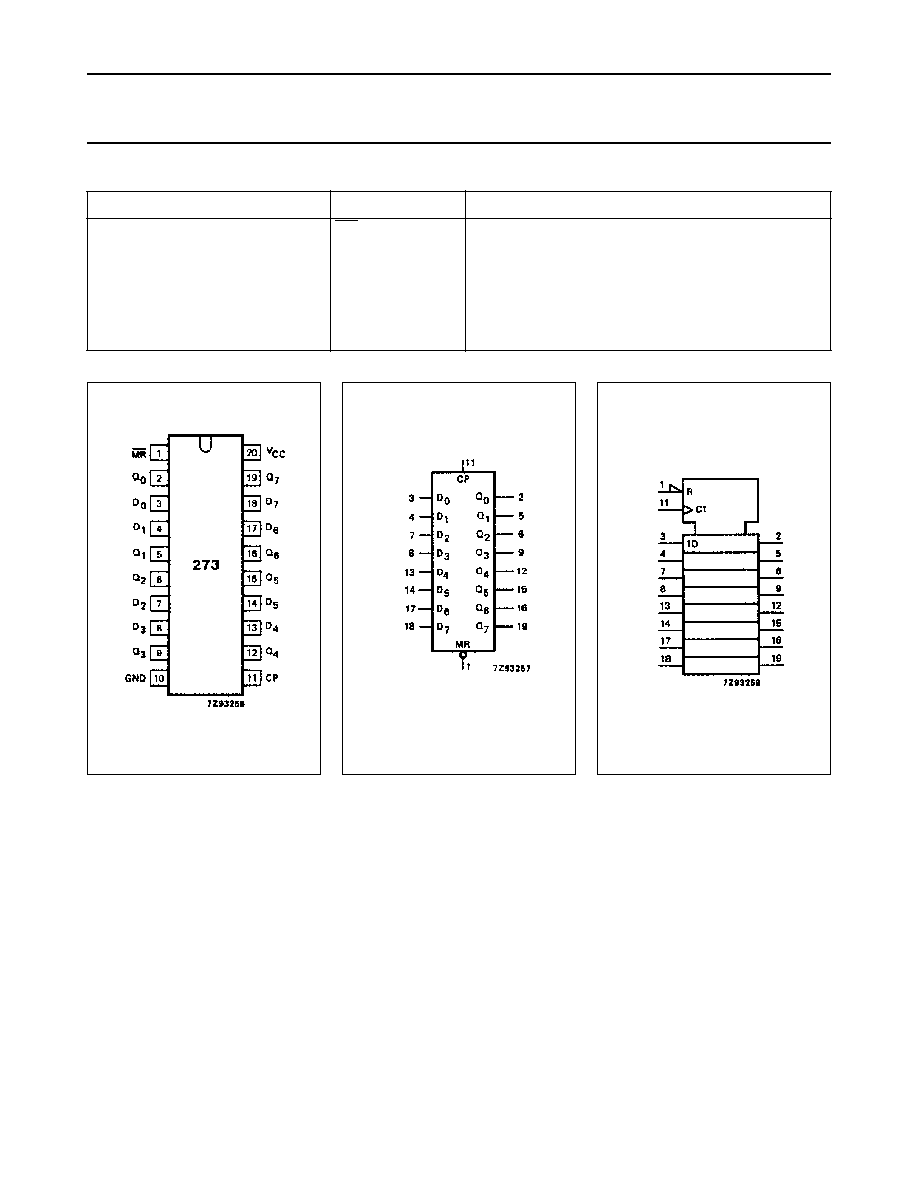
PIN DESCRIPTION
PIN NO.
SYMBOL
NAME AND FUNCTION
1
MR
master reset input (active LOW)
2, 5, 6, 9, 12, 15, 16, 19
Q
0
to Q
7
flip-flop outputs
3, 4, 7, 8, 13, 14, 17, 18
D
0
to D
7
data inputs
10
GND
ground (0 V)
11
CP
clock input (LOW-to-HIGH, edge-triggered)
20
V
CC
positive supply voltage
Fig.1 Pin configuration.
Fig.2 Logic symbol.
Fig.3 IEC logic symbol.
September 1993
4
Philips Semiconductors
Product specification
Octal D-type flip-flop with reset;
positive-edge trigger
74HC/HCT273
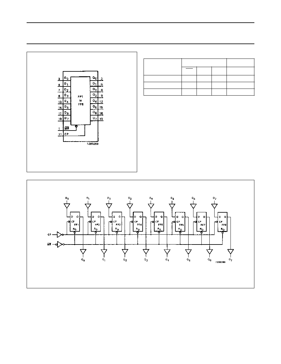
Fig.4 Functional diagram.
FUNCTION TABLE
Note
1. H = HIGH voltage level
h = HIGH voltage level one set-up time prior to the
LOW-to-HIGH CP transition
L = LOW voltage level
I = LOW voltage level one set-up time prior to the
LOW-to-HIGH CP transition
= LOW-to-HIGH transition
X = don't care
OPERATING
MODES
INPUTS
OUTPUTS
MR
CP
D
n
Q
n
reset (clear)
L
X
X
L
load "1"
H
h
H
load "0"
H
I
L
Fig.5 Logic diagram.
September 1993
5
Philips Semiconductors
Product specification
Octal D-type flip-flop with reset;
positive-edge trigger
74HC/HCT273
DC CHARACTERISTICS FOR 74HC
For the DC characteristics see
"74HC/HCT/HCU/HCMOS Logic Family Specifications"
.
Output capability: standard
I
CC
category: MSI
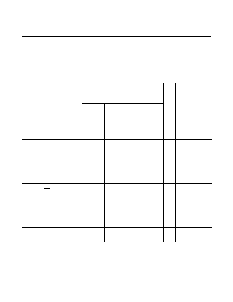
AC CHARACTERISTICS FOR 74HC
GND = 0 V; t
r
= t
f
= 6 ns; C
L
= 50 pF
SYMBOL
PARAMETER
T
amb
(
∞
C)
UNIT
TEST CONDITIONS
74HC
V
CC
(V)
WAVEFORMS
+
25
-
40 to
+
85
-
40 to
+
125
min.
typ.
max.
min.
max.
min.
max.
t
PHL
/ t
PLH
propagation delay
CP to Q
n
41
15
13
150
30
26
185
37
31
225
45
38
ns
2.0
4.5
6.0
Fig.6
t
PHL
propagation delay
MR to Q
n
44
16
14
150
30
26
185
37
31
225
45
38
ns
2.0
4.5
6.0
Fig.7
t
THL
/ t
TLH
output transition time
19
7
6
75
15
13
95
19
15
110
22
19
ns
2.0
4.5
6.0
Fig.6
t
W
clock pulse width
HIGH or LOW
80
16
14
14
5
4
100
20
17
120
24
20
ns
2.0
4.5
6.0
Fig.6
t
W
master reset pulse width
LOW
60
12
10
17
6
5
75
15
13
90
18
15
ns
2.0
4.5
6.0
Fig.7
t
rem
removal time
MR to CP
50
10
9
-
6
-
2
-
2
65
13
11
75
15
13
ns
2.0
4.5
6.0
Fig.7
t
su
set-up time
D
n
to CP
60
12
10
11
4
3
75
15
13
90
18
15
ns
2.0
4.5
6.0
Fig.8
t
h
hold time
D
n
to CP
3
3
3
-
6
-
2
-
2
3
3
3
3
3
3
ns
2.0
4.5
6.0
Fig.8
f
max
maximum clock pulse
frequency
6.0
30
35
20.6
103
122
4.8
24
28
4.0
20
24
MHz
2.0
4.5
6.0
Fig.6