
1.
General description
The 74HC283 is a high-speed Si-gate CMOS device and is pin compatible with low power
Schottky TTL (LSTTL). The 74HC283 is specified in compliance with JEDEC
standard no. 7A.
The 74HC283 adds two 4-bit binary words (An plus Bn) plus the incoming carry (CIN).
The binary sum appears on the sum outputs (S1 to S4) and the out-going carry (COUT)
according to the equation:
CIN + (A1 + B1) + 2(A2 + B2) + 4(A3 + B3) + 8(A4 + B4) =
= S1 + 2S2 + 4S3 + 8S4 + 16COUT
Where (+) = plus.
Due to the symmetry of the binary add function, the 74HC283 can be used with either all
active HIGH operands (positive logic) or all active LOW operands (negative logic). In case
of all active LOW operands the results S1 to S4 and COUT should be interpreted also as
active LOW. With active HIGH inputs, CIN must be held LOW when no carry in is
intended. Interchanging inputs of equal weight does not affect the operation, thus CIN, A1,
B1 can be assigned arbitrarily to pins 5, 6, 7, etc.
See the 74HC583 for the BCD version.
2.
Features
s
High-speed 4-bit binary addition
s
Cascadable in 4-bit increments
s
Fast internal look-ahead carry
s
Low-power dissipation
s
Complies with JEDEC standard no. 7A
s
ESD protection:
x
HBM EIA/JESD22-A114-B exceeds 2000 V
x
MM EIA/JESD22-A115-A exceeds 200 V.
s
Multiple package options
s
Specified from
-
40
�
C to +80
�
C and from
-
40
�
C to +125
�
C.
74HC283
4-bit binary full adder with fast carry
Rev. 03 -- 11 November 2004
Product data sheet

9397 750 13811
� Koninklijke Philips Electronics N.V. 2004. All rights reserved.
Product data sheet
Rev. 03 -- 11 November 2004
2 of 20
Philips Semiconductors
74HC283
4-bit binary full adder with fast carry
3.
Quick reference data
[1]
C
PD
is used to determine the dynamic power dissipation (P
D
in
�
W).
P
D
= C
PD
�
V
CC
2
�
f
i
�
N +
(C
L
�
V
CC
2
�
f
o
) where:
f
i
= input frequency in MHz;
f
o
= output frequency in MHz;
C
L
= output load capacitance in pF;
V
CC
= supply voltage in V;
N = number of inputs switching;
(C
L
�
V
CC
2
�
f
o
) = sum of outputs.
4.
Ordering information
Table 1:
Quick reference data
GND = 0 V; T
amb
= 25
�
C; t
r
= t
f
= 6 ns.
Symbol
Parameter
Conditions
Min
Typ
Max
Unit
t
PHL
, t
PLH
propagation delay
C
L
= 15 pF; V
CC
= 5 V
CIN to S1
-
16
-
ns
CIN to S2
-
18
-
ns
CIN to S3
-
20
-
ns
CIN to S4
-
23
-
ns
An or Bn to Sn
-
21
-
ns
CIN to COUT
-
20
-
ns
An or Bn to COUT
-
20
-
ns
C
I
input capacitance
-
3.5
-
pF
C
PD
power dissipation
capacitance
V
I
= GND to V
CC
[1]
-
88
-
pF
Table 2:
Ordering information
Type number
Package
Temperature range
Name
Description
Version
74HC283N
-
40
�
C to +125
�
C
DIP16
plastic dual in-line package; 16 leads (300 mil)
SOT38-4
74HC283D
-
40
�
C to +125
�
C
SO16
plastic small outline package; 16 leads;
body width 3.9 mm
SOT109-1
74HC283DB
-
40
�
C to +125
�
C
SSOP16
plastic shrink small outline package; 16 leads;
body width 5.3 mm
SOT338-1
74HC283PW
-
40
�
C to +125
�
C
TSSOP16
plastic thin shrink small outline package;
16 leads; body width 4.4 mm
SOT403-1

9397 750 13811
� Koninklijke Philips Electronics N.V. 2004. All rights reserved.
Product data sheet
Rev. 03 -- 11 November 2004
3 of 20
Philips Semiconductors
74HC283
4-bit binary full adder with fast carry
5.
Functional diagram
Fig 1.
Functional diagram
Fig 2.
Logic symbol
Fig 3.
IEC logic symbol
001aab897
CIN
A3
B3
A4
B4
S1
S2
S3
S4
A1
B1
A2
B2
14
15
12
11
4
1
13
10
5
6
3
2
9
7
COUT
001aab895
S4
S3
S2
S1
4
1
13
10
B4
A4
B3
15
A3
14
12
B2
A2
3
B1
6
2
A1
5
11
COUT
CIN
9
7
001aab896
0
3
10
13
1
4
COUT
9
0
14
3
12
3
P
Q
S
0
12
15
6
3
11
CIN
7
5

9397 750 13811
� Koninklijke Philips Electronics N.V. 2004. All rights reserved.
Product data sheet
Rev. 03 -- 11 November 2004
4 of 20
Philips Semiconductors
74HC283
4-bit binary full adder with fast carry
6.
Pinning information
6.1 Pinning
Fig 4.
Logic diagram
CIN
S1
S2
S3
S4
COUT
A1
B1
A2
B2
A3
B3
A4
B4
001aab898
Fig 5.
Pin configuration
283
S2
V
CC
B2
B3
A2
A3
S1
S3
A1
A4
B1
B4
CIN
S4
GND
COUT
001aab894
1
2
3
4
5
6
7
8
10
9
12
11
14
13
16
15

9397 750 13811
� Koninklijke Philips Electronics N.V. 2004. All rights reserved.
Product data sheet
Rev. 03 -- 11 November 2004
5 of 20
Philips Semiconductors
74HC283
4-bit binary full adder with fast carry
6.2 Pin description
7.
Functional description
7.1 Function table
[1]
H = HIGH voltage level;
L = LOW voltage level.
[2]
Example for active HIGH: 10 + 9 (0 + 1010 + 1001) = 19 (10011).
[3]
Example for active LOW: 5 + 6 (1 + 0101 + 0110) = 12 (01100).
Table 3:
Pin description
Symbol
Pin
Description
S2
1
sum output 2
B2
2
B operand input 2
A2
3
A operand input 2
S1
4
sum output 1
A1
5
A operand input 1
B1
6
B operand input 1
CIN
7
carry input
GND
8
ground (0 V)
COUT
9
carry output
S4
10
sum output 4
B4
11
B operand input 4
A4
12
A operand input 4
S3
13
sum output 3
B3
14
A operand input 3
A3
15
B operand input 3
V
CC
16
positive supply voltage
Table 4:
Function table
[1]
Pins
Input
Output
CIN
A4
A3
A2
A1
B4
B3
B2
B1
COUT
S4
S3
S2
S1
Logic levels
L
H
L
H
L
H
L
L
H
H
L
L
H
H
Active HIGH
[2]
0
1
0
1
0
1
0
0
1
1
0
0
1
1
Active LOW
[3]
1
0
1
0
1
0
1
1
0
0
1
1
0
0

9397 750 13811
� Koninklijke Philips Electronics N.V. 2004. All rights reserved.
Product data sheet
Rev. 03 -- 11 November 2004
6 of 20
Philips Semiconductors
74HC283
4-bit binary full adder with fast carry
8.
Limiting values
[1]
Above 70
�
C: P
tot
derates linearly with 12 mW/K.
[2]
Above 70
�
C: P
tot
derates linearly with 8 mW/K.
9.
Recommended operating conditions
Table 5:
Limiting values
In accordance with the Absolute Maximum Rating System (IEC 60134). Voltages are referenced to
GND (ground = 0 V).
Symbol
Parameter
Conditions
Min
Max
Unit
V
CC
supply voltage
-
0.5
+7
V
I
IK
input diode current
V
I
<
-
0.5 V or V
I
> V
CC
+ 0.5 V
-
�
20
mA
I
OK
output diode current
V
O
<
-
0.5 V or
V
O
> V
CC
+ 0.5 V
-
�
20
mA
I
O
output source or sink
current
V
O
=
-
0.5 V to V
CC
+ 0.5 V
-
�
25
mA
I
CC
, I
GND
V
CC
or GND current
-
�
50
mA
T
stg
storage temperature
-
65
+150
�
C
P
tot
power dissipation
DIP16 package
[1]
-
750
mW
SO16, SSOP16 and
TSSOP16 packages
[2]
-
500
mW
Table 6:
Recommended operating conditions
Symbol
Parameter
Conditions
Min
Typ
Max
Unit
V
CC
supply voltage
2.0
5.0
6.0
V
V
I
input voltage
0
-
V
CC
V
V
O
output voltage
0
-
V
CC
V
t
r
, t
f
input rise and fall times
V
CC
= 2.0 V
-
-
1000
ns
V
CC
= 4.5 V
-
6.0
500
ns
V
CC
= 6.0 V
-
-
400
ns
T
amb
ambient temperature
-
40
-
+125
�
C

9397 750 13811
� Koninklijke Philips Electronics N.V. 2004. All rights reserved.
Product data sheet
Rev. 03 -- 11 November 2004
7 of 20
Philips Semiconductors
74HC283
4-bit binary full adder with fast carry
10. Static characteristics
Table 7:
Static characteristics
At recommended operating conditions; voltages are referenced to GND (ground = 0 V).
Symbol
Parameter
Conditions
Min
Typ
Max
Unit
T
amb
= 25
�
C
V
IH
HIGH-level input voltage
V
CC
= 2.0 V
1.5
1.2
-
V
V
CC
= 4.5 V
3.15
2.4
-
V
V
CC
= 6.0 V
4.2
3.2
-
V
V
IL
LOW-level input voltage
V
CC
= 2.0 V
-
0.8
0.5
V
V
CC
= 4.5 V
-
2.1
1.35
V
V
CC
= 6.0 V
-
2.8
1.8
V
V
OH
HIGH-level output voltage
V
I
= V
IH
or V
IL
I
O
=
-
20
�
A; V
CC
= 2.0 V
1.9
2.0
-
V
I
O
=
-
20
�
A; V
CC
= 4.5 V
4.4
4.5
-
V
I
O
=
-
20
�
A; V
CC
= 6.0 V
5.9
6.0
-
V
I
O
=
-
4 mA; V
CC
= 4.5 V
3.98
4.32
-
V
I
O
=
-
5.2 mA; V
CC
= 6.0 V
5.48
5.81
-
V
V
OL
LOW-level output voltage
V
I
= V
IH
or V
IL
I
O
= 20
�
A; V
CC
= 2.0 V
-
0
0.1
V
I
O
= 20
�
A; V
CC
= 4.5 V
-
0
0.1
V
I
O
= 20
�
A; V
CC
= 6.0 V
-
0
0.1
V
I
O
= 4 mA; V
CC
= 4.5 V
-
0.15
0.26
V
I
O
= 5.2 mA; V
CC
= 6.0 V
-
0.16
0.26
V
I
LI
input leakage current
V
I
= V
CC
or GND; V
CC
= 6.0 V
-
-
�
0.1
�
A
I
CC
quiescent supply current
V
I
= V
CC
or GND; I
O
= 0 A;
V
CC
= 6.0 V
-
-
8.0
�
A
C
I
input capacitance
-
3.5
-
pF
T
amb
=
-
40
�
C to +85
�
C
V
IH
HIGH-level input voltage
V
CC
= 2.0 V
1.5
-
-
V
V
CC
= 4.5 V
3.15
-
-
V
V
CC
= 6.0 V
4.2
-
-
V
V
IL
LOW-level input voltage
V
CC
= 2.0 V
-
-
0.5
V
V
CC
= 4.5 V
-
-
1.35
V
V
CC
= 6.0 V
-
-
1.8
V
V
OH
HIGH-level output voltage
V
I
= V
IH
or V
IL
I
O
=
-
20
�
A; V
CC
= 2.0 V
1.9
-
-
V
I
O
=
-
20
�
A; V
CC
= 4.5 V
4.4
-
-
V
I
O
=
-
20
�
A; V
CC
= 6.0 V
5.9
-
-
V
I
O
=
-
4 mA; V
CC
= 4.5 V
3.84
-
-
V
I
O
=
-
5.2 mA; V
CC
= 6.0 V
5.34
-
-
V

9397 750 13811
� Koninklijke Philips Electronics N.V. 2004. All rights reserved.
Product data sheet
Rev. 03 -- 11 November 2004
8 of 20
Philips Semiconductors
74HC283
4-bit binary full adder with fast carry
V
OL
LOW-level output voltage
V
I
= V
IH
or V
IL
I
O
= 20
�
A; V
CC
= 2.0 V
-
-
0.1
V
I
O
= 20
�
A; V
CC
= 4.5 V
-
-
0.1
V
I
O
= 20
�
A; V
CC
= 6.0 V
-
-
0.1
V
I
O
= 4 mA; V
CC
= 4.5 V
-
-
0.33
V
I
O
= 5.2 mA; V
CC
= 6.0 V
-
-
0.33
V
I
LI
input leakage current
V
I
= V
CC
or GND; V
CC
= 6.0 V
-
-
�
1.0
�
A
I
CC
quiescent supply current
V
I
= V
CC
or GND; I
O
= 0 A;
V
CC
= 6.0 V
-
-
80
�
A
T
amb
=
-
40
�
C to +125
�
C
V
IH
HIGH-level input voltage
V
CC
= 2.0 V
1.5
-
-
V
V
CC
= 4.5 V
3.15
-
-
V
V
CC
= 6.0 V
4.2
-
-
V
V
IL
LOW-level input voltage
V
CC
= 2.0 V
-
-
0.5
V
V
CC
= 4.5 V
-
-
1.35
V
V
CC
= 6.0 V
-
-
1.8
V
V
OH
HIGH-level output voltage
V
I
= V
IH
or V
IL
-
I
O
=
-
20
�
A; V
CC
= 2.0 V
1.9
-
-
V
I
O
=
-
20
�
A; V
CC
= 4.5 V
4.4
-
-
V
I
O
=
-
20
�
A; V
CC
= 6.0 V
5.9
-
-
V
I
O
=
-
4 mA; V
CC
= 4.5 V
3.7
-
-
V
I
O
=
-
5.2 mA; V
CC
= 6.0 V
5.2
-
-
V
V
OL
LOW-level output voltage
V
I
= V
IH
or V
IL
-
I
O
= 20
�
A; V
CC
= 2.0 V
-
-
0.1
V
I
O
= 20
�
A; V
CC
= 4.5 V
-
-
0.1
V
I
O
= 20
�
A; V
CC
= 6.0 V
-
-
0.1
V
I
O
= 4 mA; V
CC
= 4.5 V
-
-
0.4
V
I
O
= 5.2 mA; V
CC
= 6.0 V
-
-
0.4
V
I
LI
input leakage current
V
I
= V
CC
or GND; V
CC
= 6.0 V
-
-
�
1.0
�
A
I
CC
quiescent supply current
V
I
= V
CC
or GND; I
O
= 0 A;
V
CC
= 6.0 V
-
-
160
�
A
Table 7:
Static characteristics
...continued
At recommended operating conditions; voltages are referenced to GND (ground = 0 V).
Symbol
Parameter
Conditions
Min
Typ
Max
Unit

9397 750 13811
� Koninklijke Philips Electronics N.V. 2004. All rights reserved.
Product data sheet
Rev. 03 -- 11 November 2004
9 of 20
Philips Semiconductors
74HC283
4-bit binary full adder with fast carry
11. Dynamic characteristics
Table 8:
Dynamic characteristics
GND = 0 V; t
r
= t
f
= 6 ns; C
L
= 50 pF; see
Figure 7
.
Symbol
Parameter
Conditions
Min
Typ
Max
Unit
T
amb
= 25
�
C
t
PHL
, t
PLH
propagation delay CIN to S1
see
Figure 6
V
CC
= 2.0 V
-
52
160
ns
V
CC
= 4.5 V
-
19
32
ns
V
CC
= 6.0 V
-
15
27
ns
V
CC
= 5.0 V; C
L
= 15 pF
-
16
-
ns
propagation delay CIN to S2
see
Figure 6
V
CC
= 2.0 V
-
58
180
ns
V
CC
= 4.5 V
-
21
36
ns
V
CC
= 6.0 V
-
17
31
ns
V
CC
= 5.0 V; C
L
= 15 pF
-
18
-
ns
propagation delay CIN to S3
see
Figure 6
V
CC
= 2.0 V
-
63
195
ns
V
CC
= 4.5 V
-
23
39
ns
V
CC
= 6.0 V
-
18
33
ns
V
CC
= 5.0 V; C
L
= 15 pF
-
20
-
ns
propagation delay CIN to S4
see
Figure 6
V
CC
= 2.0 V
-
74
230
ns
V
CC
= 4.5 V
-
27
46
ns
V
CC
= 6.0 V
-
22
39
ns
V
CC
= 5.0 V; C
L
= 15 pF
-
23
-
ns
propagation delay An or Bn to Sn
see
Figure 6
V
CC
= 2.0 V
-
69
210
ns
V
CC
= 4.5 V
-
25
42
ns
V
CC
= 6.0 V
-
20
36
ns
V
CC
= 5.0 V; C
L
= 15 pF
-
21
-
ns
propagation delay CIN to COUT
see
Figure 6
V
CC
= 2.0 V
-
63
195
ns
V
CC
= 4.5 V
-
23
39
ns
V
CC
= 6.0 V
-
18
33
ns
V
CC
= 5.0 V; C
L
= 15 pF
-
20
-
ns
propagation delay An or Bn to
COUT
see
Figure 6
V
CC
= 2.0 V
-
63
195
ns
V
CC
= 4.5 V
-
23
39
ns
V
CC
= 6.0 V
-
18
33
ns
V
CC
= 5.0 V; C
L
= 15 pF
-
20
-
ns

9397 750 13811
� Koninklijke Philips Electronics N.V. 2004. All rights reserved.
Product data sheet
Rev. 03 -- 11 November 2004
10 of 20
Philips Semiconductors
74HC283
4-bit binary full adder with fast carry
t
THL
, t
TLH
output transition time
see
Figure 6
V
CC
= 2.0 V
-
19
75
ns
V
CC
= 4.5 V
-
7
15
ns
V
CC
= 6.0 V
-
6
13
ns
C
PD
power dissipation capacitance
V
I
= GND to V
CC
[1]
-
88
-
pF
T
amb
=
-
40
�
C to +85
�
C
t
PHL
, t
PLH
propagation delay CIN to S1
see
Figure 6
V
CC
= 2.0 V
-
-
200
ns
V
CC
= 4.5 V
-
-
40
ns
V
CC
= 6.0 V
-
-
34
ns
propagation delay CIN to S2
see
Figure 6
V
CC
= 2.0 V
-
-
225
ns
V
CC
= 4.5 V
-
-
45
ns
V
CC
= 6.0 V
-
-
38
ns
propagation delay CIN to S3
see
Figure 6
V
CC
= 2.0 V
-
-
245
ns
V
CC
= 4.5 V
-
-
49
ns
V
CC
= 6.0 V
-
-
42
ns
propagation delay CIN to S4
see
Figure 6
V
CC
= 2.0 V
-
-
290
ns
V
CC
= 4.5 V
-
-
58
ns
V
CC
= 6.0 V
-
-
49
ns
propagation delay An or Bn to Sn
see
Figure 6
V
CC
= 2.0 V
-
-
265
ns
V
CC
= 4.5 V
-
-
53
ns
V
CC
= 6.0 V
-
-
45
ns
propagation delay CIN to COUT
see
Figure 6
V
CC
= 2.0 V
-
-
245
ns
V
CC
= 4.5 V
-
-
49
ns
V
CC
= 6.0 V
-
-
42
ns
propagation delay An or Bn to
COUT
see
Figure 6
V
CC
= 2.0 V
-
-
245
ns
V
CC
= 4.5 V
-
-
49
ns
V
CC
= 6.0 V
-
-
42
ns
t
THL
, t
TLH
output transition time
see
Figure 6
V
CC
= 2.0 V
-
-
95
ns
V
CC
= 4.5 V
-
-
19
ns
V
CC
= 6.0 V
-
-
16
ns
Table 8:
Dynamic characteristics
...continued
GND = 0 V; t
r
= t
f
= 6 ns; C
L
= 50 pF; see
Figure 7
.
Symbol
Parameter
Conditions
Min
Typ
Max
Unit

9397 750 13811
� Koninklijke Philips Electronics N.V. 2004. All rights reserved.
Product data sheet
Rev. 03 -- 11 November 2004
11 of 20
Philips Semiconductors
74HC283
4-bit binary full adder with fast carry
[1]
C
PD
is used to determine the dynamic power dissipation (P
D
in
�
W).
P
D
= C
PD
�
V
CC
2
�
f
i
�
N +
(C
L
�
V
CC
2
�
f
o
) where:
f
i
= input frequency in MHz;
f
o
= output frequency in MHz;
C
L
= output load capacitance in pF;
V
CC
= supply voltage in V;
N = number of inputs switching;
(C
L
�
V
CC
2
�
f
o
) sum of outputs.
T
amb
=
-
40
�
C to +125
�
C
t
PHL
, t
PLH
propagation delay CIN to S1
see
Figure 6
V
CC
= 2.0 V
-
-
240
ns
V
CC
= 4.5 V
-
-
48
ns
V
CC
= 6.0 V
-
-
41
ns
propagation delay CIN to S2
see
Figure 6
V
CC
= 2.0 V
-
-
270
ns
V
CC
= 4.5 V
-
-
54
ns
V
CC
= 6.0 V
-
-
46
ns
propagation delay CIN to S3
see
Figure 6
V
CC
= 2.0 V
-
-
295
ns
V
CC
= 4.5 V
-
-
59
ns
V
CC
= 6.0 V
-
-
50
ns
propagation delay CIN to S4
see
Figure 6
V
CC
= 2.0 V
-
-
345
ns
V
CC
= 4.5 V
-
-
69
ns
V
CC
= 6.0 V
-
-
59
ns
propagation delay An or Bn to Sn
see
Figure 6
V
CC
= 2.0 V
-
-
315
ns
V
CC
= 4.5 V
-
-
63
ns
V
CC
= 6.0 V
-
-
54
ns
propagation delay CIN to COUT
see
Figure 6
V
CC
= 2.0 V
-
-
295
ns
V
CC
= 4.5 V
-
-
59
ns
V
CC
= 6.0 V
-
-
50
ns
propagation delay An or Bn to
COUT
see
Figure 6
V
CC
= 2.0 V
-
-
295
ns
V
CC
= 4.5 V
-
-
59
ns
V
CC
= 6.0 V
-
-
50
ns
t
THL
, t
TLH
output transition time
see
Figure 6
V
CC
= 2.0 V
-
-
110
ns
V
CC
= 4.5 V
-
-
22
ns
V
CC
= 6.0 V
-
-
19
ns
Table 8:
Dynamic characteristics
...continued
GND = 0 V; t
r
= t
f
= 6 ns; C
L
= 50 pF; see
Figure 7
.
Symbol
Parameter
Conditions
Min
Typ
Max
Unit
9397 750 13811
� Koninklijke Philips Electronics N.V. 2004. All rights reserved.
Product data sheet
Rev. 03 -- 11 November 2004
12 of 20
Philips Semiconductors
74HC283
4-bit binary full adder with fast carry
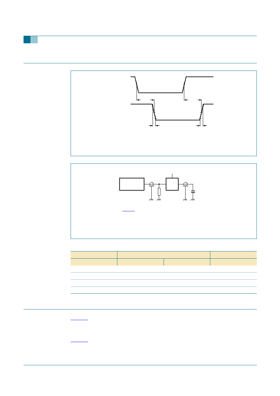
12. Waveforms
13. Application information
Figure 8
shows a 3-bit adder using the 74HC283. Trying the operand inputs of the fourth
adder (A4 and B4) LOW makes S4 dependent on, and equal to, the carry from the third
adder.
Figure 9
, based on the same principle, shows a method of dividing the 74HC283 into a
2-bit and 1-bit adder. The third stage adder (A3, B3 and S3) is used simply as means of
transferring the carry into the fourth stage (via A3 and B3) and transferring the carry from
V
M
= 0.5
�
V
I
.
Fig 6.
Waveforms showing the inputs (CIN, An and Bn) to the outputs (Sn and COUT)
propagation delays and the output transition times
Test data is given in
Table 9
.
Definitions for test circuit:
R
T
= Termination resistance should be equal to output impedance Z
o
of the pulse generator.
C
L
= Load capacitance including jig and probe capacitance.
Fig 7.
Load circuitry for switching times
Table 9:
Test data
Supply
Input
Load
V
CC
V
I
t
r
, t
f
C
L
2.0 V
V
CC
6 ns
50 pF
4.5 V
V
CC
6 ns
50 pF
6.0 V
V
CC
6 ns
50 pF
5.0 V
V
CC
6 ns
15 pF
001aab899
CIN, An, Bn,
input
Sn, COUT,
output
V
M
t
PHL
t
THL
t
TLH
t
PLH
V
M
mna101
V
CC
V
I
V
O
R
T
C
L
PULSE
GENERATOR
D.U.T.

9397 750 13811
� Koninklijke Philips Electronics N.V. 2004. All rights reserved.
Product data sheet
Rev. 03 -- 11 November 2004
13 of 20
Philips Semiconductors
74HC283
4-bit binary full adder with fast carry
the second stage on S3. As long as A3 and B3 are the same, HIGH or LOW, they do not
influence S3. Similarly, when A3 and B3 are the same, the carry into the third stage does
not influence the carry out of the third stage.
Figure 10
shows a method of implementing a 5-input encoder, where the inputs are
equally weighted. The outputs S1, S2 and S3 produce a binary number equal to the
number inputs (I1 to I5) that are HIGH.
Figure 11
shows a method of implementing a 5-input majority gate. When three or more
inputs (I1 to I5) are HIGH, the output M5 is HIGH.
Fig 8.
3-bit adder
Fig 9.
2-bit and 1-bit adder
Fig 10. 5-input encoder
Fig 11. 5-input majority gate
001aab900
S4
S3
S2
S1
C3
L
B4
A4
B3
COUT
CIN
A3
B2
A2
B1
A1
001aab901
S4
S3
S2
S1
S1
S2
C2
S10
C1
CIN
B4
A4
B3
COUT
CIN
C10
A3
A10
B2
A2
A2
B1
B1
B2
A1
A1
B10
001aab902
S4
S3
S2
S1
B4
A4
B3
COUT
CIN
I3
A3
I4
B2
A2
L
B1
I2
A1
I1
I5
001aab903
S4
S3
S2
S1
B4
A4
B3
COUT
CIN
I3
A3
I4
M5
B2
A2
B1
I2
A1
I1
I5
9397 750 13811
� Koninklijke Philips Electronics N.V. 2004. All rights reserved.
Product data sheet
Rev. 03 -- 11 November 2004
14 of 20
Philips Semiconductors
74HC283
4-bit binary full adder with fast carry
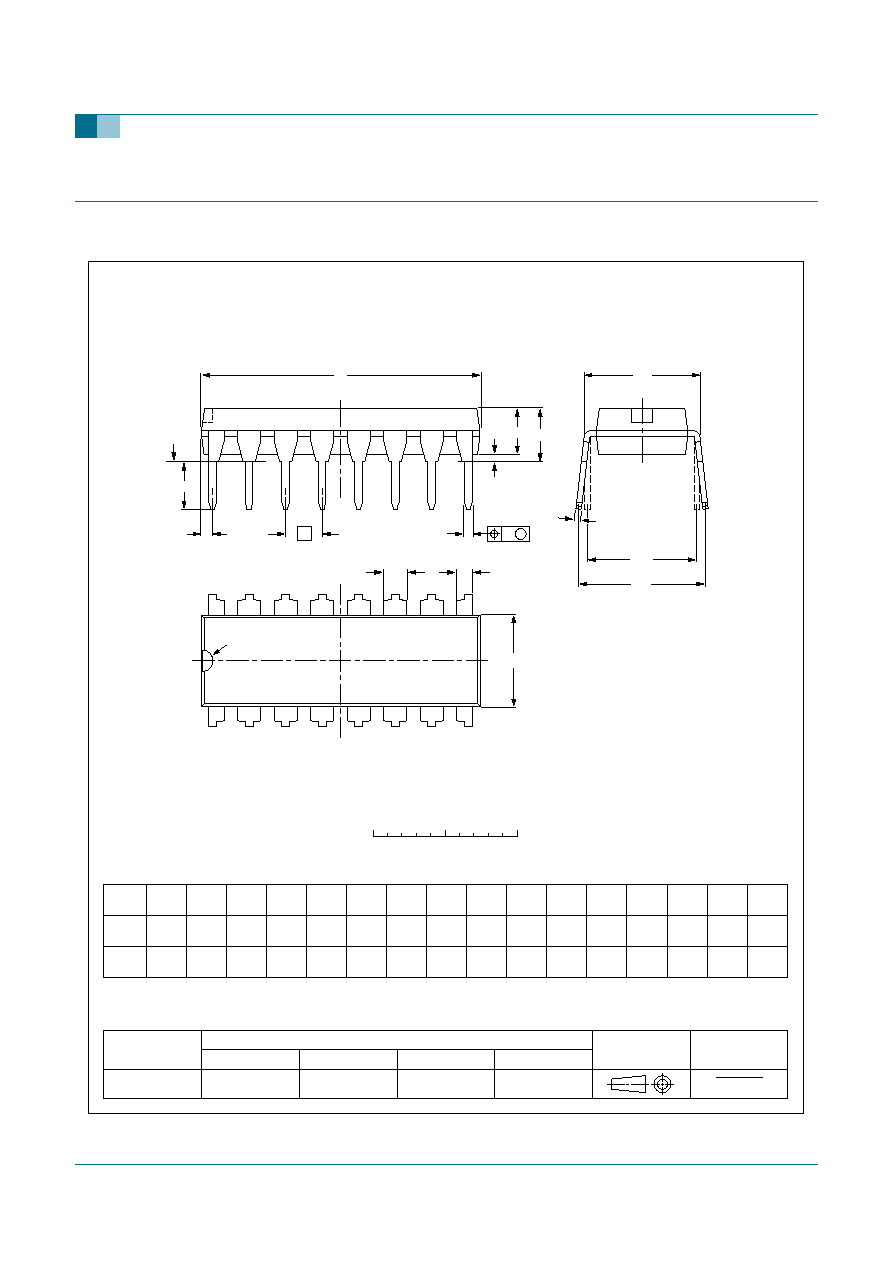
14. Package outline
Fig 12. Package outline SOT38-4 (DIP16)
REFERENCES
OUTLINE
VERSION
EUROPEAN
PROJECTION
ISSUE DATE
IEC
JEDEC
JEITA
SOT38-4
95-01-14
03-02-13
M
H
c
(e )
1
M
E
A
L
seating plane
A
1
w
M
b
1
b
2
e
D
A
2
Z
16
1
9
8
E
pin 1 index
b
0
5
10 mm
scale
Note
1. Plastic or metal protrusions of 0.25 mm (0.01 inch) maximum per side are not included.
UNIT
A
max.
1
2
b
1
(1)
(1)
(1)
b
2
c
D
E
e
M
Z
H
L
mm
DIMENSIONS (inch dimensions are derived from the original mm dimensions)
A
min.
A
max.
b
max.
w
M
E
e
1
1.73
1.30
0.53
0.38
0.36
0.23
19.50
18.55
6.48
6.20
3.60
3.05
0.254
2.54
7.62
8.25
7.80
10.0
8.3
0.76
4.2
0.51
3.2
inches
0.068
0.051
0.021
0.015
0.014
0.009
1.25
0.85
0.049
0.033
0.77
0.73
0.26
0.24
0.14
0.12
0.01
0.1
0.3
0.32
0.31
0.39
0.33
0.03
0.17
0.02
0.13
DIP16: plastic dual in-line package; 16 leads (300 mil)
SOT38-4

9397 750 13811
� Koninklijke Philips Electronics N.V. 2004. All rights reserved.
Product data sheet
Rev. 03 -- 11 November 2004
15 of 20
Philips Semiconductors
74HC283
4-bit binary full adder with fast carry
Fig 13. Package outline SOT109-1 (SO16)
X
w
M
A
A
1
A
2
b
p
D
H
E
L
p
Q
detail X
E
Z
e
c
L
v
M
A
(A )
3
A
8
9
1
16
y
pin 1 index
UNIT
A
max.
A
1
A
2
A
3
b
p
c
D
(1)
E
(1)
(1)
e
H
E
L
L
p
Q
Z
y
w
v
REFERENCES
OUTLINE
VERSION
EUROPEAN
PROJECTION
ISSUE DATE
IEC
JEDEC
JEITA
mm
inches
1.75
0.25
0.10
1.45
1.25
0.25
0.49
0.36
0.25
0.19
10.0
9.8
4.0
3.8
1.27
6.2
5.8
0.7
0.6
0.7
0.3
8
0
o
o
0.25
0.1
DIMENSIONS (inch dimensions are derived from the original mm dimensions)
Note
1. Plastic or metal protrusions of 0.15 mm (0.006 inch) maximum per side are not included.
1.0
0.4
SOT109-1
99-12-27
03-02-19
076E07
MS-012
0.069
0.010
0.004
0.057
0.049
0.01
0.019
0.014
0.0100
0.0075
0.39
0.38
0.16
0.15
0.05
1.05
0.041
0.244
0.228
0.028
0.020
0.028
0.012
0.01
0.25
0.01
0.004
0.039
0.016
0
2.5
5 mm
scale
SO16: plastic small outline package; 16 leads; body width 3.9 mm
SOT109-1

9397 750 13811
� Koninklijke Philips Electronics N.V. 2004. All rights reserved.
Product data sheet
Rev. 03 -- 11 November 2004
16 of 20
Philips Semiconductors
74HC283
4-bit binary full adder with fast carry
Fig 14. Package outline SOT338-1 (SSOP16)
UNIT
A
1
A
2
A
3
b
p
c
D
(1)
E
(1)
e
H
E
L
L
p
Q
Z
y
w
v
REFERENCES
OUTLINE
VERSION
EUROPEAN
PROJECTION
ISSUE DATE
IEC
JEDEC
JEITA
mm
0.21
0.05
1.80
1.65
0.25
0.38
0.25
0.20
0.09
6.4
6.0
5.4
5.2
0.65
1.25
7.9
7.6
1.03
0.63
0.9
0.7
1.00
0.55
8
0
o
o
0.13
0.2
0.1
DIMENSIONS (mm are the original dimensions)
Note
1. Plastic or metal protrusions of 0.25 mm maximum per side are not included.
SOT338-1
99-12-27
03-02-19
(1)
w
M
b
p
D
H
E
E
Z
e
c
v
M
A
X
A
y
1
8
16
9
A
A
1
A
2
L
p
Q
detail X
L
(A )
3
MO-150
pin 1 index
0
2.5
5 mm
scale
SSOP16: plastic shrink small outline package; 16 leads; body width 5.3 mm
SOT338-1
A
max.
2

9397 750 13811
� Koninklijke Philips Electronics N.V. 2004. All rights reserved.
Product data sheet
Rev. 03 -- 11 November 2004
17 of 20
Philips Semiconductors
74HC283
4-bit binary full adder with fast carry
Fig 15. Package outline SOT403-1 (TSSOP16)
UNIT
A
1
A
2
A
3
b
p
c
D
(1)
E
(2)
(1)
e
H
E
L
L
p
Q
Z
y
w
v
REFERENCES
OUTLINE
VERSION
EUROPEAN
PROJECTION
ISSUE DATE
IEC
JEDEC
JEITA
mm
0.15
0.05
0.95
0.80
0.30
0.19
0.2
0.1
5.1
4.9
4.5
4.3
0.65
6.6
6.2
0.4
0.3
0.40
0.06
8
0
o
o
0.13
0.1
0.2
1
DIMENSIONS (mm are the original dimensions)
Notes
1. Plastic or metal protrusions of 0.15 mm maximum per side are not included.
2. Plastic interlead protrusions of 0.25 mm maximum per side are not included.
0.75
0.50
SOT403-1
MO-153
99-12-27
03-02-18
w
M
b
p
D
Z
e
0.25
1
8
16
9
A
A
1
A
2
L
p
Q
detail X
L
(A )
3
H
E
E
c
v
M
A
X
A
y
0
2.5
5 mm
scale
TSSOP16: plastic thin shrink small outline package; 16 leads; body width 4.4 mm
SOT403-1
A
max.
1.1
pin 1 index

9397 750 13811
� Koninklijke Philips Electronics N.V. 2004. All rights reserved.
Product data sheet
Rev. 03 -- 11 November 2004
18 of 20
Philips Semiconductors
74HC283
4-bit binary full adder with fast carry
15. Revision history
Table 10:
Revision history
Document ID
Release
date
Data sheet status
Change notice Doc. number
Supersedes
74HC283_3
20041111
Product data sheet
-
9397 750 13811
74HC_HCT283_CNV_2
Modifications:
�
The format of this data sheet has been redesigned to comply with the current presentation
and information standard of Philips Semiconductors.
�
Removed type number 74HCT283.
�
Inserted family specification.
74HC_HCT283_CNV_2
19970828
Product specification -
-
74HC_HCT283_1
74HC_HCT283_1
19901201
Product specification -
-
-

Philips Semiconductors
74HC283
4-bit binary full adder with fast carry
9397 750 13811
� Koninklijke Philips Electronics N.V. 2004. All rights reserved.
Product data sheet
Rev. 03 -- 11 November 2004
19 of 20
16. Data sheet status
[1]
Please consult the most recently issued data sheet before initiating or completing a design.
[2]
The product status of the device(s) described in this data sheet may have changed since this data sheet was published. The latest information is available on the Internet at
URL http://www.semiconductors.philips.com.
[3]
For data sheets describing multiple type numbers, the highest-level product status determines the data sheet status.
17. Definitions
Short-form specification -- The data in a short-form specification is
extracted from a full data sheet with the same type number and title. For
detailed information see the relevant data sheet or data handbook.
Limiting values definition -- Limiting values given are in accordance with
the Absolute Maximum Rating System (IEC 60134). Stress above one or
more of the limiting values may cause permanent damage to the device.
These are stress ratings only and operation of the device at these or at any
other conditions above those given in the Characteristics sections of the
specification is not implied. Exposure to limiting values for extended periods
may affect device reliability.
Application information -- Applications that are described herein for any
of these products are for illustrative purposes only. Philips Semiconductors
make no representation or warranty that such applications will be suitable for
the specified use without further testing or modification.
18. Disclaimers
Life support -- These products are not designed for use in life support
appliances, devices, or systems where malfunction of these products can
reasonably be expected to result in personal injury. Philips Semiconductors
customers using or selling these products for use in such applications do so
at their own risk and agree to fully indemnify Philips Semiconductors for any
damages resulting from such application.
Right to make changes -- Philips Semiconductors reserves the right to
make changes in the products - including circuits, standard cells, and/or
software - described or contained herein in order to improve design and/or
performance. When the product is in full production (status `Production'),
relevant changes will be communicated via a Customer Product/Process
Change Notification (CPCN). Philips Semiconductors assumes no
responsibility or liability for the use of any of these products, conveys no
license or title under any patent, copyright, or mask work right to these
products, and makes no representations or warranties that these products are
free from patent, copyright, or mask work right infringement, unless otherwise
specified.
19. Contact information
For additional information, please visit: http://www.semiconductors.philips.com
For sales office addresses, send an email to: sales.addresses@www.semiconductors.philips.com
Level
Data sheet status
[1]
Product status
[2] [3]
Definition
I
Objective data
Development
This data sheet contains data from the objective specification for product development. Philips
Semiconductors reserves the right to change the specification in any manner without notice.
II
Preliminary data
Qualification
This data sheet contains data from the preliminary specification. Supplementary data will be published
at a later date. Philips Semiconductors reserves the right to change the specification without notice, in
order to improve the design and supply the best possible product.
III
Product data
Production
This data sheet contains data from the product specification. Philips Semiconductors reserves the
right to make changes at any time in order to improve the design, manufacturing and supply. Relevant
changes will be communicated via a Customer Product/Process Change Notification (CPCN).

� Koninklijke Philips Electronics N.V. 2004
All rights are reserved. Reproduction in whole or in part is prohibited without the prior
written consent of the copyright owner. The information presented in this document does
not form part of any quotation or contract, is believed to be accurate and reliable and may
be changed without notice. No liability will be accepted by the publisher for any
consequence of its use. Publication thereof does not convey nor imply any license under
patent- or other industrial or intellectual property rights.
Date of release: 11 November 2004
Document number: 9397 750 13811
Published in The Netherlands
Philips Semiconductors
74HC283
4-bit binary full adder with fast carry
20. Contents
1
General description . . . . . . . . . . . . . . . . . . . . . . 1
2
Features . . . . . . . . . . . . . . . . . . . . . . . . . . . . . . . 1
3
Quick reference data . . . . . . . . . . . . . . . . . . . . . 2
4
Ordering information . . . . . . . . . . . . . . . . . . . . . 2
5
Functional diagram . . . . . . . . . . . . . . . . . . . . . . 3
6
Pinning information . . . . . . . . . . . . . . . . . . . . . . 4
6.1
Pinning . . . . . . . . . . . . . . . . . . . . . . . . . . . . . . . 4
6.2
Pin description . . . . . . . . . . . . . . . . . . . . . . . . . 5
7
Functional description . . . . . . . . . . . . . . . . . . . 5
7.1
Function table . . . . . . . . . . . . . . . . . . . . . . . . . . 5
8
Limiting values. . . . . . . . . . . . . . . . . . . . . . . . . . 6
9
Recommended operating conditions. . . . . . . . 6
10
Static characteristics. . . . . . . . . . . . . . . . . . . . . 7
11
Dynamic characteristics . . . . . . . . . . . . . . . . . . 9
12
Waveforms . . . . . . . . . . . . . . . . . . . . . . . . . . . . 12
13
Application information. . . . . . . . . . . . . . . . . . 12
14
Package outline . . . . . . . . . . . . . . . . . . . . . . . . 14
15
Revision history . . . . . . . . . . . . . . . . . . . . . . . . 18
16
Data sheet status . . . . . . . . . . . . . . . . . . . . . . . 19
17
Definitions . . . . . . . . . . . . . . . . . . . . . . . . . . . . 19
18
Disclaimers . . . . . . . . . . . . . . . . . . . . . . . . . . . . 19
19
Contact information . . . . . . . . . . . . . . . . . . . . 19