 | –≠–ª–µ–∫—Ç—Ä–æ–Ω–Ω—ã–π –∫–æ–º–ø–æ–Ω–µ–Ω—Ç: 74HC299PW | –°–∫–∞—á–∞—Ç—å:  PDF PDF  ZIP ZIP |

DATA SHEET
Product specification
File under Integrated Circuits, IC06
December 1990
INTEGRATED CIRCUITS
74HC/HCT299
8-bit universal shift register; 3-state
For a complete data sheet, please also download:
∑
The IC06 74HC/HCT/HCU/HCMOS Logic Family Specifications
∑
The IC06 74HC/HCT/HCU/HCMOS Logic Package Information
∑
The IC06 74HC/HCT/HCU/HCMOS Logic Package Outlines

December 1990
2
Philips Semiconductors
Product specification
8-bit universal shift register; 3-state
74HC/HCT299
FEATURES
∑
Multiplexed inputs/outputs provide improved bit density
∑
Four operating modes:
≠ shift left
≠ shift right
≠ hold (store)
≠ load data
∑
Operates with output enable or at high-impedance
OFF-state (Z)
∑
3-state outputs drive bus lines directly
∑
Can be cascaded for n-bits word length
∑
Output capability: bus driver (parallel I/Os),
standard (serial outputs)
∑
I
CC
category: MSI
GENERAL DESCRIPTION
The 74HC/HCT299 are high-speed Si-gate CMOS devices
and are pin compatible with low power Schottky TTL
(LSTTL). They are specified in compliance with JEDEC
standard no. 7A.
The 74HC/HCT299 contain eight edge-triggered D-type
flip-flops and the interstage logic necessary to perform
synchronous shift-right, shift-left, parallel load and hold
operations. The type of operation is determined by the
mode select inputs (S
0
and S
1
), as shown in the mode
select table.
All flip-flop outputs have 3-state buffers to separate these
outputs (I/O
0
to I/O
7
) such, that they can serve as data
inputs in the parallel load mode. The serial outputs (Q
0
and
Q
7
) are used for expansion in serial shifting of longer
words.
A LOW signal on the asynchronous master reset input
(MR) overrides the S
n
and clock (CP) inputs and resets the
flip-flops. All other state changes are initiated by the rising
edge of the clock pulse. Inputs can change when the clock
is either state, provided that the recommended set-up and
hold times, relative to the rising edge of CP, are observed.
A HIGH signal on the 3-state output enable inputs (OE
1
or
OE
2
) disables the 3-state buffers and the I/O
n
outputs are
set to the high-impedance OFF-state. In this condition, the
shift, hold, load and reset operations can still occur. The
3-state buffers are also disabled by HIGH signals on both
S
0
and S
1
, when in preparation for a parallel load
operation.
QUICK REFERENCE DATA
GND = 0 V; T
amb
= 25
∞
C; t
r
= t
f
= 6 ns
SYMBOL
PARAMETER
CONDITIONS
TYPICAL
UNIT
HC
HCT
t
PHL/
t
PLH
propagation delay
C
L
= 15 pF; V
CC
= 5 V
CP to Q
0
, Q
7
20
19
ns
CP to I/O
n
20
19
ns
t
PHL
MR to Q
0
, Q
7
or I/O
n
20
23
ns
f
max
maximum clock frequency
50
46
MHz
C
I
input capacitance
3.5
3.5
pF
C
I/O
input/output capacitance
10
10
pF
C
PD
power dissipation capacitance per package
notes 1 and 2
120
125
pF
Notes
1. C
PD
is used to determine the dynamic power
dissipation (P
D
in
µ
W):
P
D
= C
PD
◊
V
CC
2
◊
f
i
+
(C
L
◊
V
CC
2
◊
f
o
) where:
f
i
= input frequency in MHz
f
o
= output frequency in MHz
(C
L
◊
V
CC
2
◊
f
o
) = sum of outputs
C
L
= output load capacitance in pF
V
CC
= supply voltage in V
2. For HC the condition is V
I
= GND to V
CC
For HCT the condition is V
I
= GND to V
CC
-
1.5 V
ORDERING INFORMATION
See
"74HC/HCT/HCU/HCMOS Logic Package
Information"
.
December 1990
3
Philips Semiconductors
Product specification
8-bit universal shift register; 3-state
74HC/HCT299
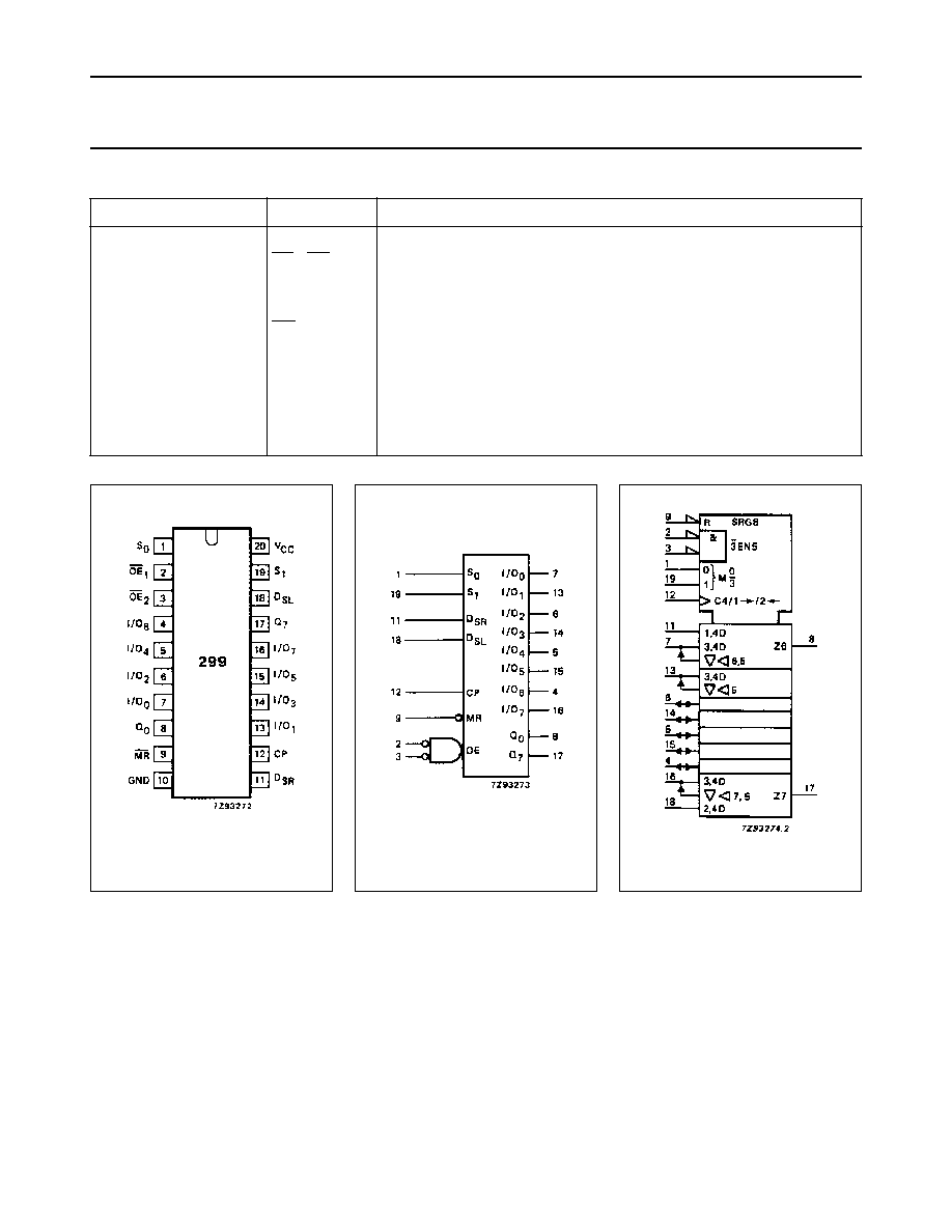
PIN DESCRIPTION
PIN NO.
SYMBOL
NAME AND FUNCTION
1, 19
S
0
, S
1
mode select inputs
2, 3
OE
1
, OE
2
3-state output enable inputs (active LOW)
7, 13, 6, 14, 5, 15, 4, 16
I/O
0
to I/O
7
parallel data inputs or 3-state parallel outputs (bus driver)
8, 17
Q
0
, Q
7
serial outputs (standard output)
9
MR
asynchronous master reset input (active LOW)
10
GND
ground (0 V)
11
D
SR
serial data shift-right input
12
CP
clock input (LOW-to-HIGH, edge-triggered)
18
D
SL
serial data shift-left input
20
V
CC
positive supply voltage
Fig.1 Pin configuration.
Fig.2 Logic symbol.
Fig.3 IEC logic symbol.
December 1990
4
Philips Semiconductors
Product specification
8-bit universal shift register; 3-state
74HC/HCT299
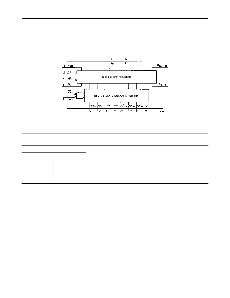
MODE SELECT TABLE
Notes
1. H = HIGH voltage level
L = LOW voltage level
X = don't care
= LOW-to-HIGH CP transition
INPUTS
RESPONSE
MR
S
1
S
0
CP
L
X
X
X
asynchronous reset; Q
0
-
Q
7
= LOW
H
H
H
H
H
L
H
L
H
H
L
L
X
parallel load; I/O
n
Q
n
shift right; D
SR
Q
0
, Q
0
Q
1
etc.
shift left; D
SL
Q
7
, Q
7
Q
6
etc.
hold
Fig.4 Functional diagram.
December 1990
5
Philips Semiconductors
Product specification
8-bit universal shift register; 3-state
74HC/HCT299
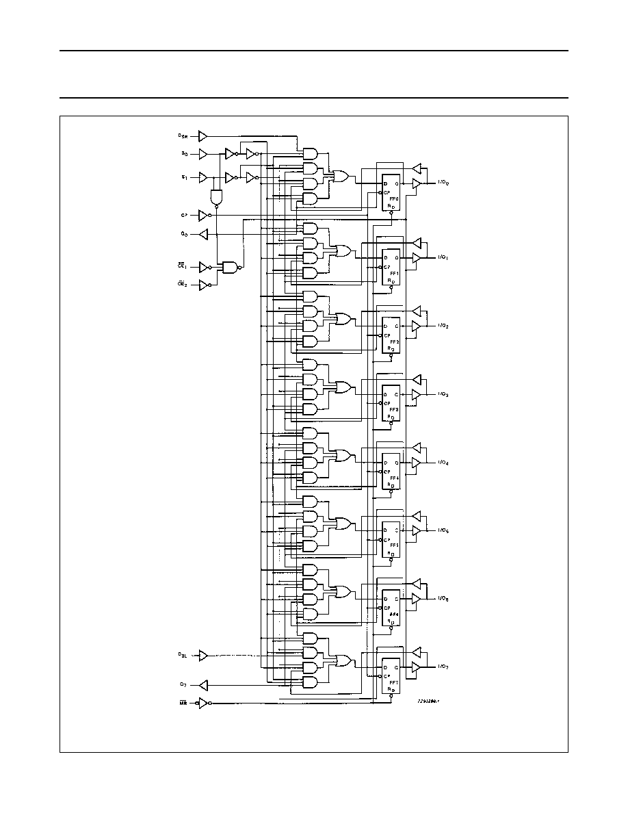
Fig.5 Logic diagram.

December 1990
6
Philips Semiconductors
Product specification
8-bit universal shift register; 3-state
74HC/HCT299
DC CHARACTERISTICS FOR 74HC
For the DC characteristics see
"74HC/HCT/HCU/HCMOS Logic Family Specifications"
.
Output capability: bus driver (parallel I/Os)
standard (serial outputs)
I
CC
category: MSI
AC CHARACTERISTICS FOR 74HC
GND = 0 V; t
r
= t
f
= 6 ns; C
L
= 50 pF
SYMBOL
PARAMETER
T
amb
(
∞
C)
UNIT
TEST CONDITIONS
74HC
V
CC
(V)
WAVEFORMS
+
25
-
40 to
+
85
-
40 to
+
125
min. typ.
max.
min.
max.
min.
max.
t
PHL
/ t
PLH
propagation delay
CP to Q
0
, Q
7
66
24
19
200
40
34
250
50
43
300
60
51
ns
2.0
4.5
6.0
Fig.6
t
PHL
/ t
PLH
propagation delay
CP to I/O
n
66
24
19
200
40
34
250
50
43
300
60
51
ns
2.0
4.5
6.0
Fig.6
t
PHL
/
propagation delay
MR to Q
0
, Q
7
or I/O
n
66
24
19
200
40
34
250
50
43
300
60
51
ns
2.0
4.5
6.0
Fig.7
t
PZH
3-state output enable time
OE
n
to I/O
n
50
18
14
155
31
26
195
39
33
235
47
40
ns
2.0
4.5
6.0
Fig.9
t
PZL
3-state output enable time
OE
n
to I/O
n
41
15
12
130
26
22
165
33
28
195
39
33
ns
2.0
4.5
6.0
Fig.9
t
PHZ
3-state output disable time
OE
n
to I/O
n
66
24
19
185
37
31
230
46
39
280
56
48
ns
2.0
4.5
6.0
Fig.9
t
PLZ
3-state output disable time
OE
n
to I/O
n
55
20
16
155
31
26
195
39
33
235
47
40
ns
2.0
4.5
6.0
Fig.9
t
THL
/ t
TLH
output transition time
bus driver (I/O
n
)
14
5
4
60
12
10
75
15
13
90
18
15
ns
2.0
4.5
6.0
Fig.6
t
THL
/ t
TLH
output transition time
standard (Q
0
, Q
7
)
19
7
6
75
15
13
95
19
16
110
22
19
ns
2.0
4.5
6.0
Fig.6
t
W
clock pulse width
HIGH or LOW
80
16
14
17
6
5
100
20
17
120
24
20
ns
2.0
4.5
6.0
Fig.6
t
W
master reset pulse width
LOW
80
16
14
19
7
6
100
20
17
120
24
20
ns
2.0
4.5
6.0
Fig.7
December 1990
7
Philips Semiconductors
Product specification
8-bit universal shift register; 3-state
74HC/HCT299
t
rem
removal time
MR to CP
5
5
5
-14
-
5
-
4
5
5
5
5
5
5
ns
2.0
4.5
6.0
Fig.7
t
su
set-up time
D
SR
, D
SL
to CP
100
20
17
33
12
10
125
25
21
150
30
26
ns
2.0
4.5
6.0
Fig.6
t
su
set-up time
S
0
, S
1
to CP
100
20
17
33
12
10
125
25
21
150
30
26
ns
2.0
4.5
6.0
Fig.8
t
su
set-up time
I/O
n
to CP
125
25
21
39
14
11
155
31
26
190
38
32
ns
2.0
4.5
6.0
Fig.6
t
h
hold time
I/O
n
, D
SR
, D
SL
to CP
0
0
0
-
14
-
5
-
4
0
0
0
0
0
0
ns
2.0
4.5
6.0
Fig.6
t
h
hold time
S
0
, S
1
to CP
0
0
0
-
28
-
10
-
8
0
0
0
0
0
0
ns
2.0
4.5
6.0
Fig.8
f
max
maximum clock pulse
frequency
5.0
25
29
15
45
54
4.0
20
24
3.4
17
20
MHz
2.0
4.5
6.0
Fig.6
SYMBOL
PARAMETER
T
amb
(
∞
C)
UNIT
TEST CONDITIONS
74HC
V
CC
(V)
WAVEFORMS
+
25
-
40 to
+
85
-
40 to
+
125
min. typ.
max.
min.
max.
min.
max.

December 1990
8
Philips Semiconductors
Product specification
8-bit universal shift register; 3-state
74HC/HCT299
DC CHARACTERISTICS FOR 74HCT
For the DC characteristics see
"74HC/HCT/HCU/HCMOS Logic Family Specifications"
.
Output capability: bus driver (parallel I/Os)
standard (serial outputs)
I
CC
category: MSI
Note to HCT types
The value of additional quiescent supply current (
I
CC
) for unit load of 1 is given in the family specifications.
To determine
I
CC
per input, multiply this value by the unit load coefficient shown in the table below.
INPUT
UNIT LOAD COEFFICIENT
I/O
n
D
SR
, D
SL
CP, S
0
MR, S
1
OE
n
0.25
0.25
0.60
0.25
0.30

December 1990
9
Philips Semiconductors
Product specification
8-bit universal shift register; 3-state
74HC/HCT299
AC CHARACTERISTICS FOR 74HCT
GND = 0 V; t
r
= t
f
= 6 ns; C
L
= 50 pF
SYMBOL PARAMETER
T
amb
(
∞
C)
UNIT
TEST CONDITIONS
74HCT
V
CC
(V)
WAVEFORMS
+
25
-
40 to
+
85
-
40 to
+
125
min.
typ.
max.
min.
max.
min.
max.
t
PHL
/ t
PLH
propagation delay
CP to Q
0
, Q
7
22
37
46
56
ns
4.5
Fig.6
t
PHL
/ t
PLH
propagation delay
CP to I/O
n
22
37
46
56
ns
4.5
Fig.6
t
PHL
propagation delay
MR to Q
0
, Q
7
or I/O
n
27
46
58
69
ns
4.5
Fig.7
t
PZH
/ t
PZL
3-state output enable time
OE
n
to I/O
n
19
30
38
45
ns
4.5
Fig.9
t
PHZ
3-state output disable time
OE
n
to I/O
n
24
37
46
56
ns
4.5
Fig.9
t
PLZ
3-state output disable time
OE
n
to I/O
n
20
32
40
48
ns
4.5
Fig.9
t
THL
/ t
TLH
output transition time
bus driver (I/O
n
)
5
12
15
18
ns
4.5
Fig.6
t
THL
/ t
TLH
output transition time
standard (Q
0
, Q
7
)
7
15
19
22
ns
4.5
Fig.6
t
W
clock pulse width
HIGH or LOW
20
10
25
30
ns
4.5
Fig.6
t
W
master reset pulse width
LOW
20
11
25
30
ns
4.5
Fig.7
t
rem
removal time
MR to CP
10
2
9
11
ns
4.5
Fig.7
t
su
set-up time
I/O
n
, D
SR
, D
SL
to CP
25
14
31
38
ns
4.5
Fig.6
t
su
set-up time
S
0
, S
1
to CP
32
18
40
48
ns
4.5
Fig.8
t
h
hold time
I/O
n
, D
SR
, D
SL
to CP
0
-
11
0
0
ns
4.5
Fig.6
t
h
hold time
S
0
, S
1
to CP
0
-
17
0
0
ns
4.5
Fig.8
f
max
maximum clock pulse
frequency
25
42
20
17
MHz
4.5
Fig.6
December 1990
10
Philips Semiconductors
Product specification
8-bit universal shift register; 3-state
74HC/HCT299
AC WAVEFORMS
handbook, full pagewidth
MBA335
1/ f max
VM
(1)
t su
t h
t su
t h
VM
(1)
t W
t PHL
VM
(1)
t
THL
t PLH
t
TLH
I/O ,D ,D
n
SR
SL
INPUTS
CP INPUT
I/O ,Q ,Q
OUTPUTS
n
0
7
Fig.6
Waveforms showing the clock (CP) to output (I/O
n
, Q
0
, Q
7
) propagation delays, the clock pulse width, the
I/O
n
, D
SR
and D
SL
to CP set-up and hold times, the output transition times and the maximum clock
frequency.
The shaded areas indicate when the input is
permitted to change for predictable output
performance.
(1) HC : V
M
= 50%; V
I
= GND to V
CC
.
HCT : V
M
= 1.3 V; V
I
= GND to 3 V.
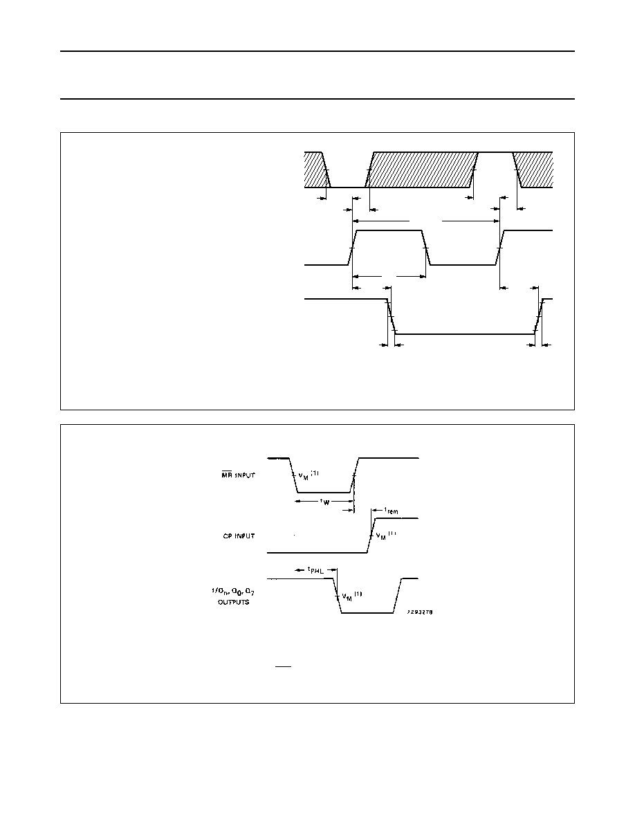
Fig.7
Waveforms showing the master reset (MR) pulse width (LOW), the master reset to output (I/O
n
, Q
0
, Q
7
)
propagation delays and the master reset to clock (CP) removal time.
(1) HC : V
M
= 50%; V
I
= GND to V
CC
.
HCT : V
M
= 1.3 V; V
I
= GND to 3 V.
December 1990
11
Philips Semiconductors
Product specification
8-bit universal shift register; 3-state
74HC/HCT299
PACKAGE OUTLINES
See
"74HC/HCT/HCU/HCMOS Logic Package Outlines"
.
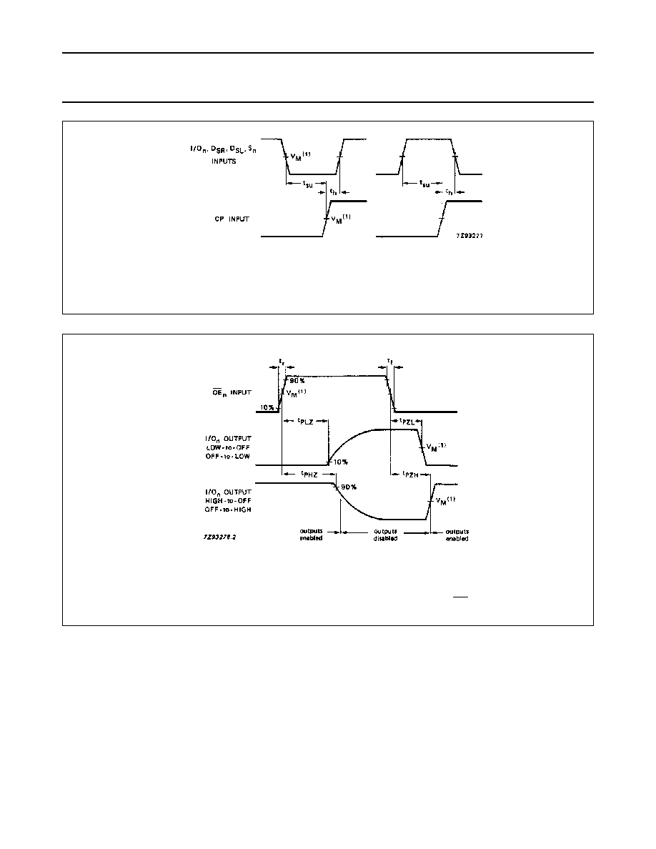
Fig.8
Waveforms showing the set-up and hold times from the mode control inputs (S
0
, S
1
) to the clock (CP).
(1) HC : V
M
= 50%; V
I
= GND to V
CC
.
HCT : V
M
= 1.3 V; V
I
= GND to 3 V.
Fig.9 Waveforms showing the 3-state enable and disable times for OE
n
inputs.
(1) HC : V
M
= 50%; V
I
= GND to V
CC
.
HCT : V
M
= 1.3 V; V
I
= GND to 3 V.