2003 Feb 12
2
Philips Semiconductors
Product specification
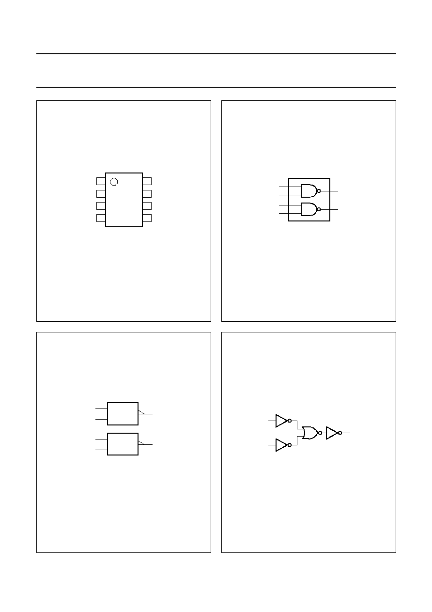
Dual 2-input NAND gate
74HC2G00; 74HCT2G00
FEATURES
∑
Wide supply voltage range from 2.0 to 6.0 V
∑
Symmetrical output impedance
∑
High noise immunity
∑
Low power dissipation
∑
Balanced propagation delays
∑
Very small 8 pins package
∑
Output capability is standard
∑
ESD protection:
HBM EIA/JESD22-A114-A exceeds 2000 V
MM EIA/JESD22-A115-A exceeds 200 V.
DESCRIPTION
The 74HC2G/HCT2G00 is a high-speed Si-gate CMOS
device.
The 74HC2G/HCT2G00 provides the 2-input NAND
function.
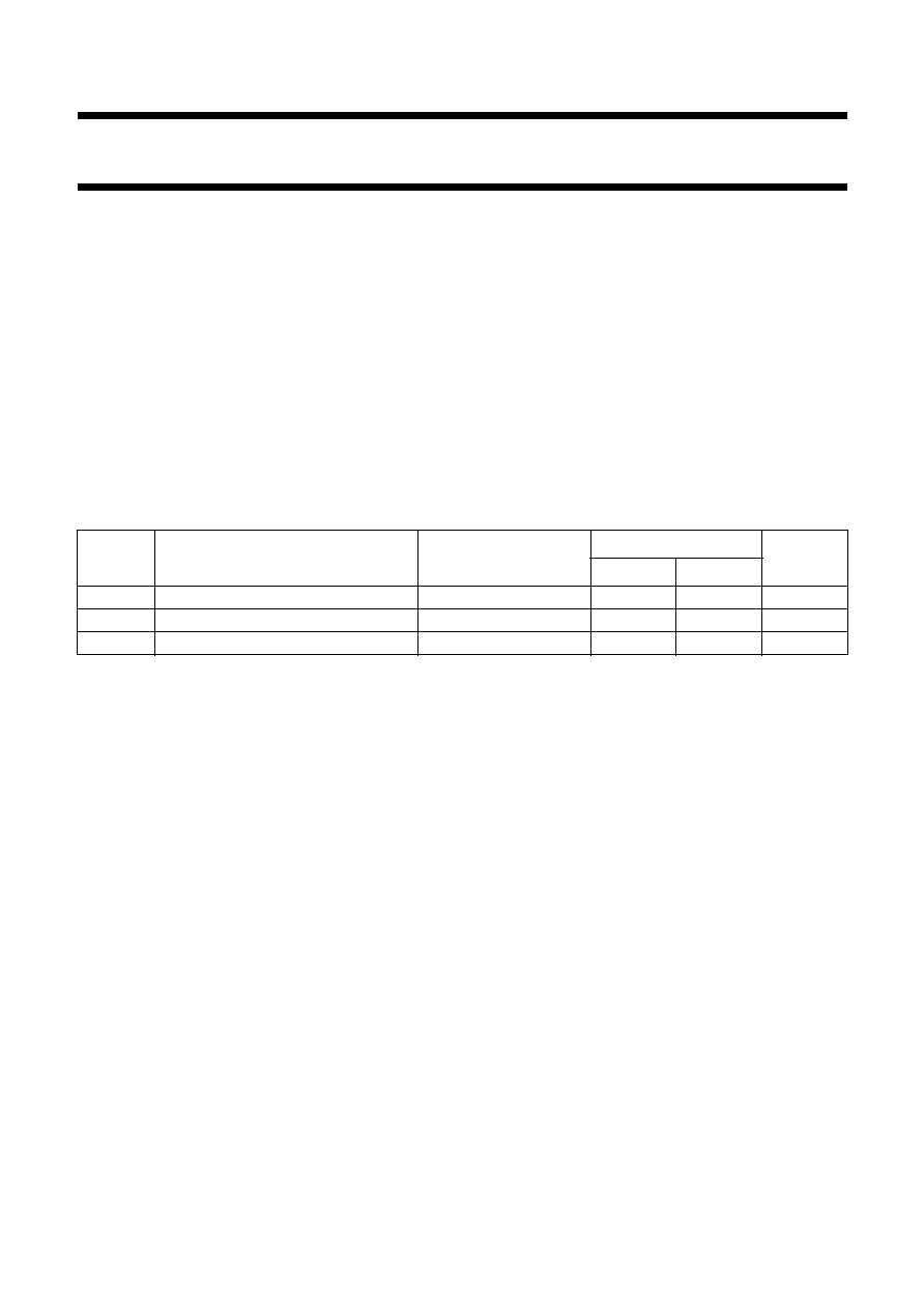
QUICK REFERENCE DATA
GND = 0 V; T
amb
= 25
∞
C; t
r
= t
f
6.0 ns.
Notes
1. C
PD
is used to determine the dynamic power dissipation (P
D
in
µ
W).
P
D
= C
PD
◊
V
CC
2
◊
f
i
◊
N +
(C
L
◊
V
CC
2
◊
f
o
) where:
f
i
= input frequency in MHz;
f
o
= output frequency in MHz;
C
L
= output load capacitance in pF;
N = total load switching outputs;
V
CC
= supply voltage in Volts;
(C
L
◊
V
CC
2
◊
f
o
) = sum of outputs.
2. For 74HC2G00 the condition is V
I
= GND to V
CC
.
For 74HCT2G00 the condition is V
I
= GND to V
CC
-
1.5 V.
SYMBOL
PARAMETER
CONDITIONS
TYPICAL
UNIT
HC2G00
HCT2G00
t
PHL
/t
PLH
propagation delay nA, nB to nY
C
L
= 50 pF; V
CC
= 4.5 V
9
12
ns
C
I
input capacitance
1.5
1.5
pF
C
PD
power dissipation capacitance per gate notes 1 and 2
10
10
pF
2003 Feb 12
5
Philips Semiconductors
Product specification
Dual 2-input NAND gate
74HC2G00; 74HCT2G00
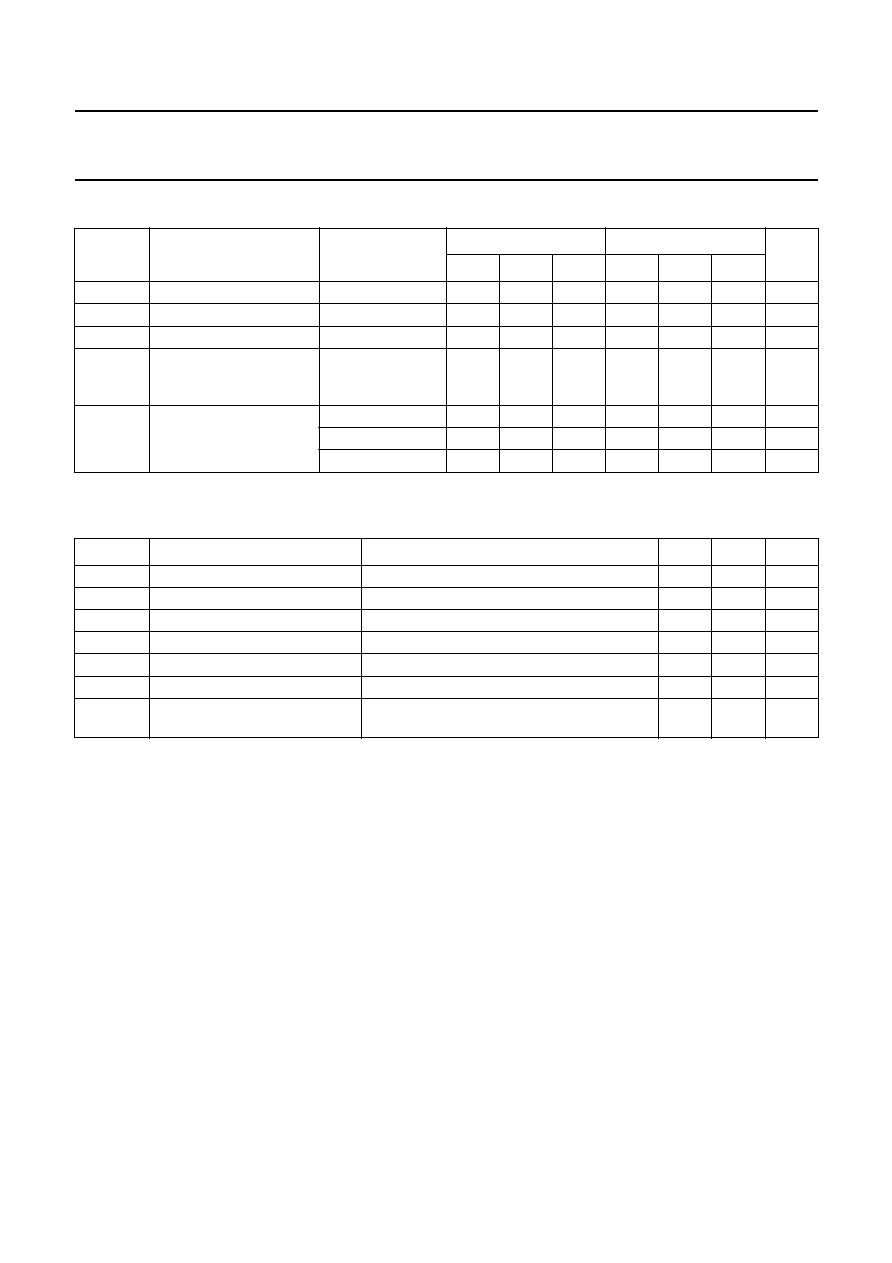
RECOMMENDED OPERATING CONDITIONS
LIMITING VALUES
In accordance with the Absolute Maximum Rating System (IEC 60134); voltages are referenced to GND (ground = 0 V).
Notes
1. The input and output voltage ratings may be exceeded if the input and output current ratings are observed.
2. Above 110
∞
C the value of P
D
derates linearly with 8 mW/K.
SYMBOL
PARAMETER
CONDITIONS
74HC2G00
74HCT2G00
UNIT
MIN.
TYP.
MAX.
MIN.
TYP.
MAX.
V
CC
supply voltage
2.0
5.0
6.0
4.5
5.0
5.5
V
V
I
input voltage
0
-
V
CC
0
-
V
CC
V
V
O
output voltage
0
-
V
CC
0
-
V
CC
V
T
amb
operating ambient
temperature
see DC and AC
characteristics per
device
-
40
+25
+125
-
40
+25
+125
∞
C
t
r
, t
f
input rise and fall times
V
CC
= 2.0 V
-
-
1000
-
-
-
ns
V
CC
= 4.5 V
-
6.0
500
-
6.0
500
ns
V
CC
= 6.0 V
-
-
400
-
-
-
ns
SYMBOL
PARAMETER
CONDITIONS
MIN.
MAX.
UNIT
V
CC
supply voltage
-
0.5
+7.0
V
I
IK
input diode current
V
I
<
-
0.5 V or V
I
> V
CC
+ 0.5 V; note 1
-
±
20
mA
I
OK
output diode current
V
O
<
-
0.5 V or V
O
> V
CC
+ 0.5 V; note 1
-
±
20
mA
I
O
output source or sink current
-
0.5 V < V
O
< V
CC
+ 0.5 V; note 1
-
25
mA
I
CC
V
CC
or GND current
note 1
-
50
mA
T
stg
storage temperature
-
65
+150
∞
C
P
D
power dissipation per package
for temperature range from
-
40 to +125
∞
C;
note 2
-
300
mW