2003 May 1
2
Philips Semiconductors
Preliminary specification
Inverting Schmitt-triggers
74HC2G14; 74HCT2G14
FEATURES
∑
Wide supply voltage range from 2.0 to 6.0 V
∑
High noise immunity
∑
Low power dissipation
∑
Balanced propagation delays
∑
Unlimited input rise and fall times
∑
Very small 6 pins package.
APPLICATIONS
∑
Wave and pulse shapers for highly noisy environments
∑
Astable multivibrators
∑
Monostable multivibrators
∑
Output capability: standard.
DESCRIPTION
The 74HC2G/HCT2G14 is a high-speed Si-gate CMOS
device.
The 74HC2G/HCT2G14 provides two inverting buffers
with Schmitt-trigger action. This device is capable of
transforming slowly changing input signals into sharply
defined, jitter-free output signals.
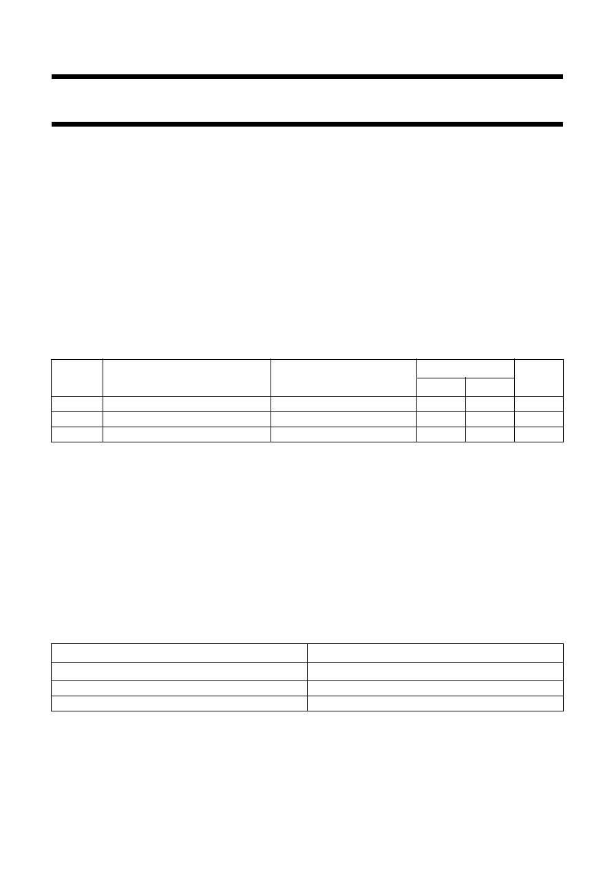
QUICK REFERENCE DATA
GND = 0 V; T
amb
= 25
∞
C; t
r
= t
f
6.0 ns.
Notes
1. C
PD
is used to determine the dynamic power dissipation (P
D
in
µ
W).
P
D
= C
PD
◊
V
CC
2
◊
f
i
◊
N +
(C
L
◊
V
CC
2
◊
f
o
) where:
f
i
= input frequency in MHz; f
o
= output frequency in MHz;
C
L
= output load capacitance in pF;
V
CC
= supply voltage in Volts;
N = total switching outputs;
(C
L
◊
V
CC
2
◊
f
o
) = sum of outputs.
2. For HC2G the condition is V
I
= GND to V
CC
.
For HCT2G the condition is V
I
= GND to V
CC
-
1.5 V.
FUNCTION TABLE
See note 1.
Note
1. H = HIGH voltage level;
L = LOW voltage level.
SYMBOL
PARAMETER
CONDITIONS
TYPICAL
UNIT
HC2G
HCT2G
t
PHL
/t
PLH
propagation delay nA to nY
C
L
= 50 pF; V
CC
= 4.5 V
16
21
ns
C
I
input capacitance
2
2
pF
C
PD
power dissipation capacitance
notes 1 and 2
10
10
pF
INPUTS
OUTPUTS
nA
nY
L
H
H
L
2003 May 1
4
Philips Semiconductors
Preliminary specification
Inverting Schmitt-triggers
74HC2G14; 74HCT2G14
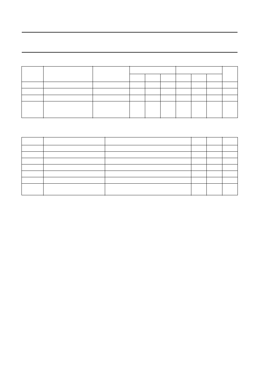
RECOMMENDED OPERATING CONDITIONS
LIMITING VALUES
In accordance with the Absolute Maximum Rating System (IEC 60134); voltages are referenced to GND (ground = 0 V).
Notes
1. The input and output voltage ratings may be exceeded if the input and output current ratings are observed.
2. Above 110
∞
C the value of P
D
derates linearly with 8 mW/K.
SYMBOL
PARAMETER
CONDITIONS
74HC2G14
74HCT2G14
UNIT
MIN.
TYP.
MAX.
MIN.
TYP.
MAX.
V
CC
supply voltage
2.0
5.0
6.0
4.5
5.0
5.5
V
V
I
input voltage
0
-
V
CC
0
-
V
CC
V
V
O
output voltage
0
-
V
CC
0
-
V
CC
V
T
amb
operating ambient
temperature
see DC and AC
characteristics per
device
-
40
+25
+125
-
40
+25
+125
∞
C
SYMBOL
PARAMETER
CONDITIONS
MIN.
MAX.
UNIT
V
CC
supply voltage
-
0.5
+7.0
V
I
IK
input diode current
V
I
<
-
0.5 V or V
I
> V
CC
+ 0.5 V; note 1
-
±
20
mA
I
OK
output diode current
V
O
<
-
0.5 V or V
O
> V
CC
+ 0.5 V; note 1
-
±
20
mA
I
O
output source or sink current
-
0.5 V < V
O
< V
CC
+ 0.5 V; note 1
-
25
mA
I
CC
V
CC
or GND current
note 1
-
50
mA
T
stg
storage temperature
-
65
+150
∞
C
P
D
power dissipation per package
for temperature range from
-
40 to +125
∞
C;
note 2
-
300
mW
2003 May 1
5
Philips Semiconductors
Preliminary specification
Inverting Schmitt-triggers
74HC2G14; 74HCT2G14
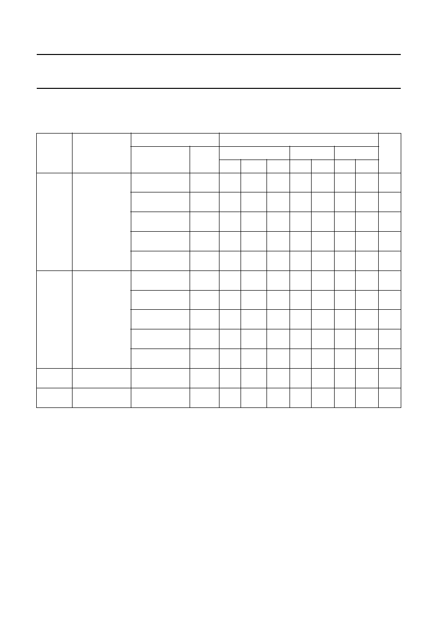
DC CHARACTERISTICS
Type 74HC2G14
At recommended operating conditions; voltages are referenced to GND (ground = 0 V).
Note
1. All typical values are measured at T
amb
= 25
∞
C.
SYMBOL
PARAMETER
TEST CONDITIONS
T
amb
(
∞
C)
UNIT
OTHER
V
CC
(V)
+25
-
40 to +85
-
40 to +125
MIN. TYP.
(1)
MAX. MIN. MAX. MIN. MAX.
V
OH
HIGH-level
output voltage
V
I
= V
IH
or V
IL
:
I
O
=
-
20
µ
A
2.0
1.9
2.0
-
1.9
-
1.9
-
V
V
I
= V
IH
or V
IL
:
I
O
=
-
20
µ
A
4.5
4.4
4.5
-
4.4
-
4.4
-
V
V
I
= V
IH
or V
IL
:
I
O
=
-
20
µ
A
6.0
5.9
6.0
-
5.9
-
5.9
-
V
V
I
= V
IH
or V
IL
;
I
O
=
-
4.0 mA
4.5
4.18
4.32
-
4.13
-
3.7
-
V
V
I
= V
IH
or V
IL
;
I
O
=
-
5.2 mA
6.0
5.68
5.81
-
5.63
-
5.2
-
V
V
OL
LOW-level output
voltage
V
I
= V
IH
or V
IL
;
I
O
= 20
µ
A
2.0
-
0
0.1
-
0.1
-
0.1
V
V
I
= V
IH
or V
IL
;
I
O
= 20
µ
A
4.5
-
0
0.1
-
0.1
-
0.1
V
V
I
= V
IH
or V
IL
;
I
O
= 20
µ
A
6.0
-
0
0.1
-
0.1
-
0.1
V
V
I
= V
IH
or V
IL
;
I
O
= 4.0 mA
4.5
-
0.15
0.26
-
0.33
-
0.4
V
V
I
= V
IH
or V
IL
;
I
O
= 5.2 mA
6.0
-
0.16
0.26
-
0.33
-
0.4
V
I
I
input leakage
current
V
I
= V
CC
or GND
6.0
-
-
±
0.1
-
±
1.0
-
±
1.0
µ
A
I
CC
quiescent supply
current
V
I
= V
CC
or GND;
I
O
= 0
6.0
-
-
1.0
-
10
-
20
µ
A

