2003 Aug 29
2
Philips Semiconductors
Product specification
Quad 2-input OR gate
74HC32; 74HCT32
FEATURES
·
Wide supply voltage range from 2.0 to 6.0 V
·
Symmetrical output impedance
·
High noise immunity
·
Low power dissipation
·
Balanced propagation delays
·
ESD protection:
HBM EIA/JESD22-A114-A exceeds 2000 V
MM EIA/JESD22-A115-A exceeds 200 V.
GENERAL DESCRIPTION
The 74HC/HCT32 is a high-speed Si-gate CMOS device
and is pin compatible with low power Schottky TTL
(LSTTL). They are specified in compliance with JEDEC
standard no. 7A.
The 74HC/HCT32 provides the 2-input OR function.
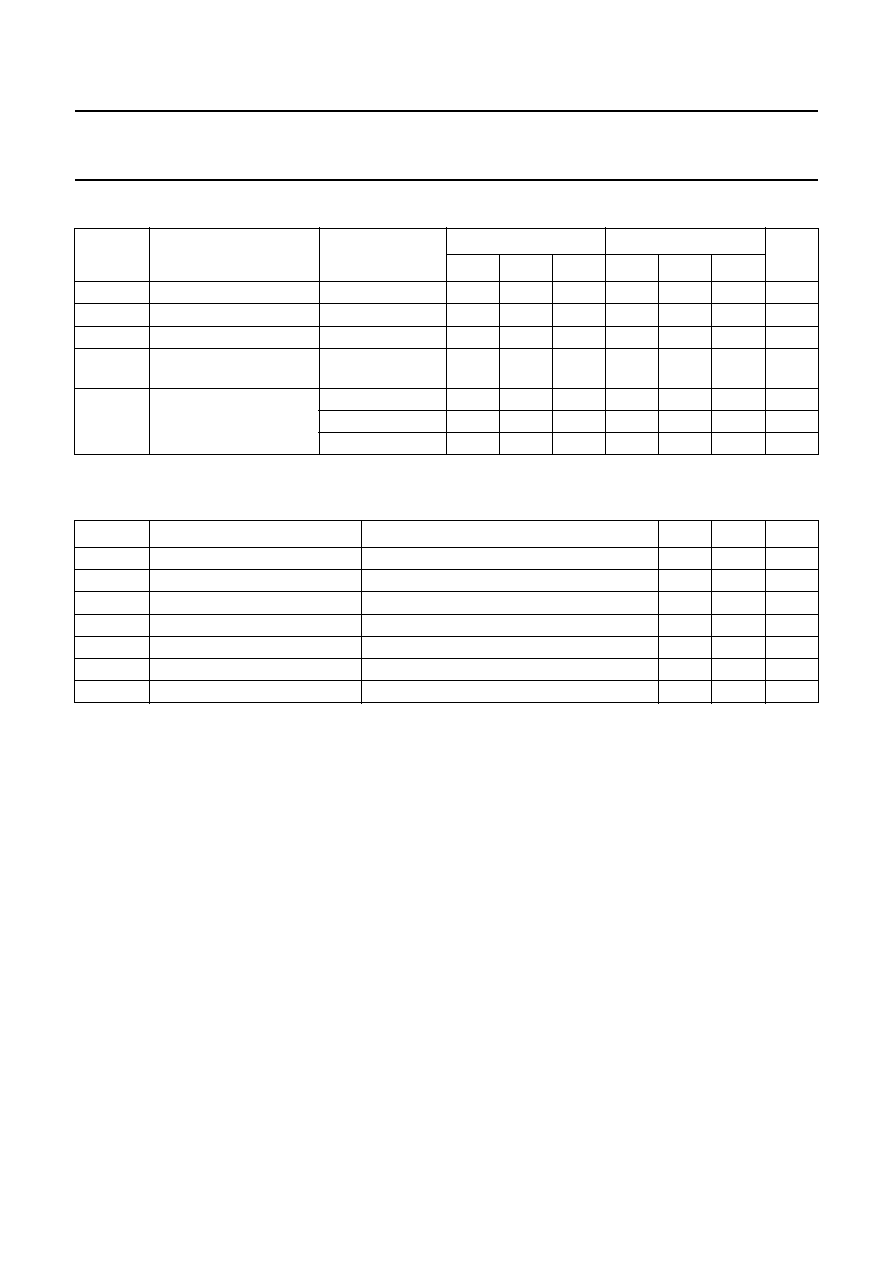
QUICK REFERENCE DATA
GND = 0 V; T
amb
= 25
°
C; t
r
= t
f
= 6 ns.
Notes
1. C
PD
is used to determine the dynamic power dissipation (P
D
in
µ
W).
P
D
= C
PD
×
V
CC
2
×
f
i
×
N +
(C
L
×
V
CC
2
×
f
o
) where:
f
i
= input frequency in MHz;
f
o
= output frequency in MHz;
C
L
= output load capacitance in pF;
V
CC
= supply voltage in Volts;
N = total load switching outputs;
(C
L
×
V
CC
2
×
f
o
) = sum of the outputs.
2. For 74HC32 the condition is V
I
= GND to V
CC
.
For 74HCT32 the condition is V
I
= GND to V
CC
-
1.5 V.
FUNCTION TABLE
See note 1.
Note
1. H = HIGH voltage level;
L = LOW voltage level.
SYMBOL
PARAMETER
CONDITIONS
TYPICAL
UNIT
HC
HCT
t
PHL
/t
PLH
propagation delay nA, nB to nY
C
L
= 15 pF; V
CC
= 5 V
6
9
ns
C
I
input capacitance
3.5
3.5
pF
C
PD
power dissipation capacitance per gate
notes 1 and 2
16
28
pF
INPUT
OUTPUT
nA
nB
nY
L
L
L
L
H
H
H
L
H
H
H
H
2003 Aug 29
4
Philips Semiconductors
Product specification
Quad 2-input OR gate
74HC32; 74HCT32
handbook, halfpage
1
14
GND
(1)
1A
VCC
7
2
3
4
5
6
1B
1Y
2A
2B
2Y
13
12
11
10
9
4B
4A
4Y
3B
3A
8
GND
Top view
3Y
MNB060
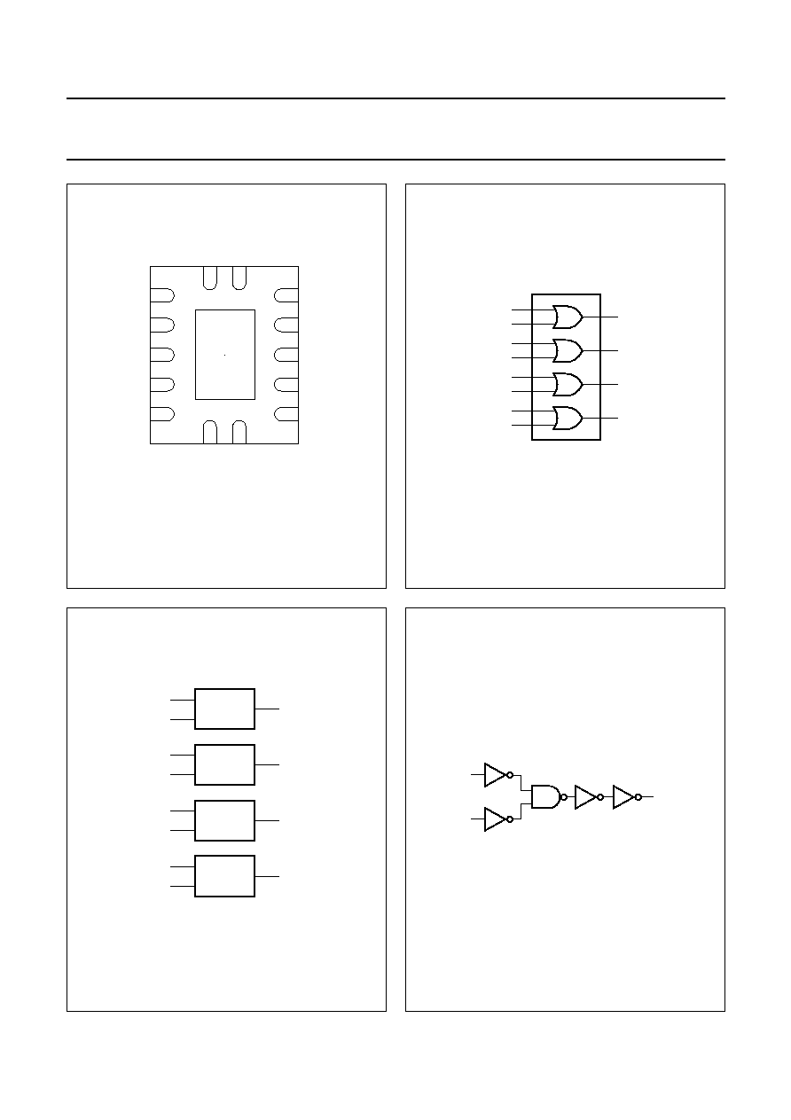
Fig.2 Pin configuration DHVQFN14.
(1) The die substrate is attached to this pad using conductive die
attach material. It can not be used as a supply pin or input.
handbook, halfpage
MNA242
1A
1B
1Y
2
1
3
2A
2B
2Y
5
4
6
3A
3B
3Y
10
9
8
4A
4B
4Y
13
12
11
Fig.3 Logic symbol.
handbook, halfpage
MNA243
3
1
1
1
1
2
1
6
5
4
8
10
9
11
13
12
Fig.4 Logic symbol (IEEE/IEC).
handbook, halfpage
MNA241
A
B
Y
Fig.5 Logic diagram (one gate).
2003 Aug 29
5
Philips Semiconductors
Product specification
Quad 2-input OR gate
74HC32; 74HCT32
RECOMMENDED OPERATING CONDITIONS
LIMITING VALUES
In accordance with the Absolute Maximum Rating System (IEC 60134); voltages are referenced to GND (ground = 0 V).
Notes
1. The input and output voltage ratings may be exceeded if the input and output current ratings are observed.
2. For DIP14 packages: above 70
°
C the value of P
D
derates linearly with 12 mW/K.
For SO14 packages: above 70
°
C the value of P
D
derates linearly with 8 mW/K.
For SSOP14 and TSSOP14 packages: above 60
°
C the value of P
D
derates linearly with 5.5 mW/K.
For DHVQFN14 packages: above 60
°
C the value of P
D
derates linearly with 4.5 mW/K.
SYMBOL
PARAMETER
CONDITIONS
74HC32
74HCT32
UNIT
MIN.
TYP.
MAX.
MIN.
TYP.
MAX.
V
CC
supply voltage
2.0
5.0
6.0
4.5
5.0
5.5
V
V
I
input voltage
0
-
V
CC
0
-
V
CC
V
V
O
output voltage
0
-
V
CC
0
-
V
CC
V
T
amb
operating ambient
temperature
-
40
+25
+125
-
40
+25
+125
°
C
t
r
, t
f
input rise and fall times
V
CC
= 2.0 V
-
-
1000
-
-
-
ns
V
CC
= 4.5 V
-
6.0
500
-
6.0
500
ns
V
CC
= 6.0 V
-
-
400
-
-
-
ns
SYMBOL
PARAMETER
CONDITIONS
MIN.
MAX.
UNIT
V
CC
supply voltage
-
0.5
+7.0
V
I
IK
input diode current
V
I
<
-
0.5 V or V
I
> V
CC
+ 0.5 V; note 1
-
±
20
mA
I
OK
output diode current
V
O
<
-
0.5 V or V
O
> V
CC
+ 0.5 V; note 1
-
±
20
mA
I
O
output source or sink current
-
0.5 V < V
O
< V
CC
+ 0.5 V; note 1
-
±
25
mA
I
CC
; I
GND
V
CC
or GND current
note 1
-
±
50
mA
T
stg
storage temperature
-
65
+150
°
C
P
D
power dissipation
T
amb
=
-
40 to +125
°
C; note 2
-
300
mW