 | –≠–ª–µ–∫—Ç—Ä–æ–Ω–Ω—ã–π –∫–æ–º–ø–æ–Ω–µ–Ω—Ç: 74HC368 | –°–∫–∞—á–∞—Ç—å:  PDF PDF  ZIP ZIP |
DATA SHEET
Product specification
File under Integrated Circuits, IC06
December 1990
INTEGRATED CIRCUITS
74HC/HCT368
Hex buffer/line driver; 3-state;
inverting
For a complete data sheet, please also download:
∑
The IC06 74HC/HCT/HCU/HCMOS Logic Family Specifications
∑
The IC06 74HC/HCT/HCU/HCMOS Logic Package Information
∑
The IC06 74HC/HCT/HCU/HCMOS Logic Package Outlines
December 1990
2
Philips Semiconductors
Product specification
Hex buffer/line driver; 3-state; inverting
74HC/HCT368
FEATURES
∑
Inverting outputs
∑
Output capability: bus driver
∑
I
CC
category: MSI
GENERAL DESCRIPTION
The 74HC/HCT368 are high-speed Si-gate CMOS devices
and are pin compatible with low power Schottky TTL
(LSTTL). They are specified in compliance with JEDEC
standard no. 7A.
The 74HC/HCT368 are hex inverting buffer/line drivers
with 3-state outputs. The 3-state outputs (nY) are
controlled by the output enable inputs (1OE, 2OE).
A HIGH on nOE causes the outputs to assume a high
impedance OFF-state.
The "368" is identical to the "367" but has inverting outputs.
QUICK REFERENCE DATA
GND = 0 V; T
amb
= 25
∞
C; t
r
= t
f
= 6 ns
Notes
1. C
PD
is used to determine the dynamic power dissipation (P
D
in
µ
W):
P
D
= C
PD
◊
V
CC
2
◊
f
i
+
(C
L
◊
V
CC
2
◊
f
o
) where:
f
i
= input frequency in MHz
f
o
= output frequency in MHz
(C
L
◊
V
CC
2
◊
f
o
) = sum of outputs
C
L
= output load capacitance in pF
V
CC
= supply voltage in V
2. For HC the condition is V
I
= GND to V
CC
For HCT the condition is V
I
= GND to V
CC
-
1.5 V
ORDERING INFORMATION
See
"74HC/HCT/HCU/HCMOS Logic Package Information"
.
SYMBOL
PARAMETER
CONDITIONS
TYPICAL
UNIT
HC
HCT
t
PHL
/ t
PLH
propagation delay nA to nY
C
L
= 15 pF; V
CC
= 5 V
9
11
ns
C
I
input capacitance
3.5
3.5
pF
C
PD
power dissipation capacitance per buffer
notes 1 and 2
30
30
pF
December 1990
3
Philips Semiconductors
Product specification
Hex buffer/line driver; 3-state; inverting
74HC/HCT368
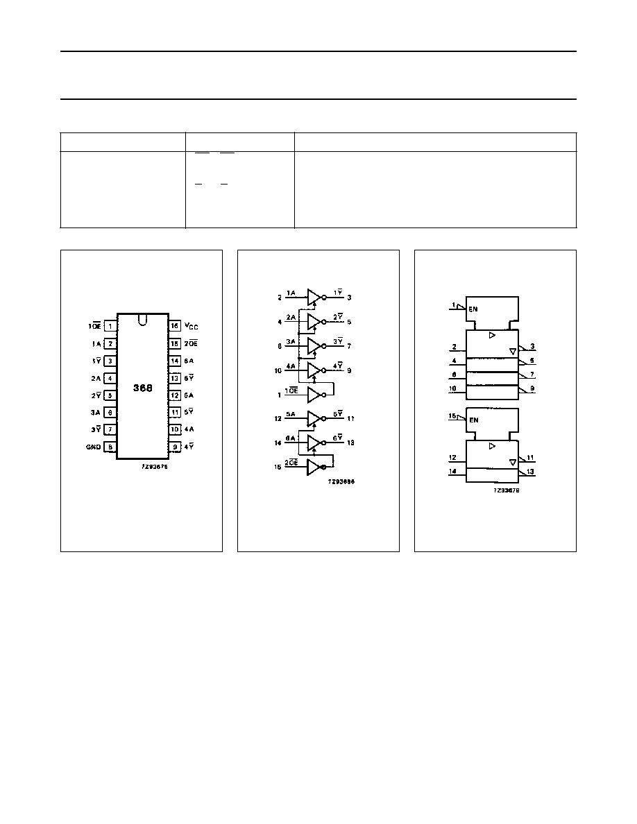
PIN DESCRIPTION
PIN NO.
SYMBOL
NAME AND FUNCTION
1, 15
1OE, 2OE
output enable inputs (active LOW)
2, 4, 6, 10, 12, 14
1A to 6A
data inputs
3, 5, 7, 9, 11, 13
1Y to 6Y
data outputs
8
GND
ground (0 V)
16
V
CC
positive supply voltage
Fig.1 Pin configuration.
Fig.2 Logic symbol.
Fig.3 IEC logic symbol.
December 1990
4
Philips Semiconductors
Product specification
Hex buffer/line driver; 3-state; inverting
74HC/HCT368
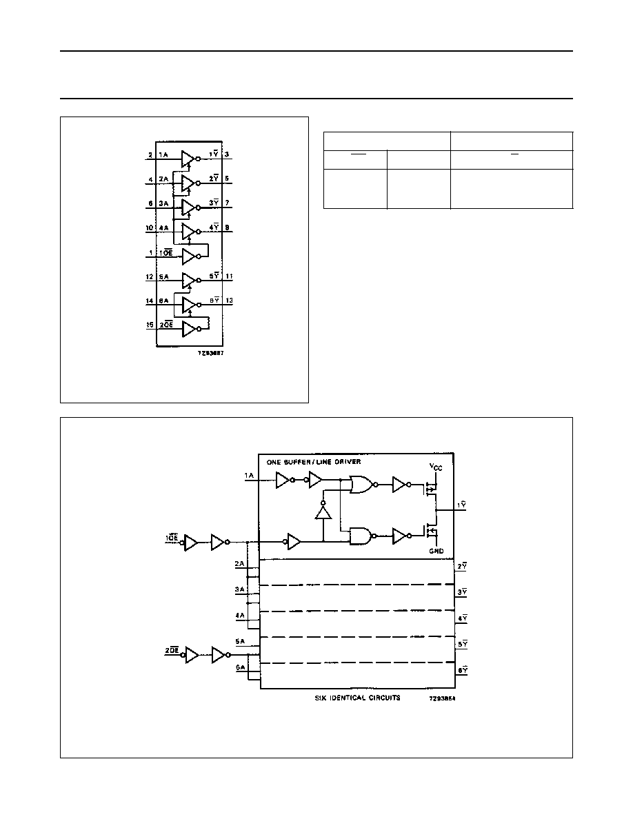
Fig.4 Functional diagram.
FUNCTION TABLE
Note
1. H = HIGH voltage level
L = LOW voltage level
X = don't care
Z = high impedance OFF-state
INPUTS
OUTPUTS
nOE
nA
nY
L
L
H
L
H
X
H
L
Z
Fig.5 Logic diagram.
December 1990
5
Philips Semiconductors
Product specification
Hex buffer/line driver; 3-state; inverting
74HC/HCT368
DC CHARACTERISTICS FOR 74HC
For the DC characteristics see
"74HC/HCT/HCU/HCMOS Logic Family Specifications"
.
Output capability: bus driver
I
CC
category: MSI
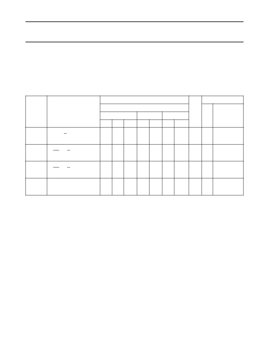
AC CHARACTERISTICS FOR 74HC
GND = 0 V; t
r
= t
f
= 6 ns; C
L
= 50 pF
SYMBOL
PARAMETER
T
amb
(
∞
C)
UNIT
TEST CONDITIONS
74HC
V
CC
(V)
WAVEFORMS
+
25
-
40 to
+
85
-
40 to
+
125
min.
typ.
max. min. max. min.
max.
t
PHL
/ t
PLH
propagation delay
nA to nY
30
11
9
95
19
16
120
24
20
145
29
25
ns
2.0
4.5
6.0
Fig.6
t
PZH
/ t
PZL
3-state output enable time
nOE to nY
41
15
12
150
30
26
190
38
33
225
45
38
ns
2.0
4.5
6.0
Fig.7
t
PHZ
/ t
PLZ
3-state output disable time
nOE to nY
55
20
16
150
30
26
190
38
33
225
45
38
ns
2.0
4.5
6.0
Fig.7
t
THL
/ t
TLH
output transition time
14
5
4
60
12
10
75
15
13
90
18
15
ns
2.0
4.5
6.0
Fig.6