 | –≠–ª–µ–∫—Ç—Ä–æ–Ω–Ω—ã–π –∫–æ–º–ø–æ–Ω–µ–Ω—Ç: 74HC393U | –°–∫–∞—á–∞—Ç—å:  PDF PDF  ZIP ZIP |
Document Outline
- FEATURES
- GENERAL DESCRIPTION
- QUICK REFERENCE DATA
- ORDERING INFORMATION
- PIN DESCRIPTION
- COUNT SEQUENCE
- DC CHARACTERISTICS
- AC CHARACTERISTICS
- AC WAVEFORMS
- PACKAGE OUTLINES

DATA SHEET
Product specification
File under Integrated Circuits, IC06
December 1990
INTEGRATED CIRCUITS
74HC/HCT393
Dual 4-bit binary ripple counter
For a complete data sheet, please also download:
∑
The IC06 74HC/HCT/HCU/HCMOS Logic Family Specifications
∑
The IC06 74HC/HCT/HCU/HCMOS Logic Package Information
∑
The IC06 74HC/HCT/HCU/HCMOS Logic Package Outlines

December 1990
2
Philips Semiconductors
Product specification
Dual 4-bit binary ripple counter
74HC/HCT393
FEATURES
∑
Two 4-bit binary counters with individual clocks
∑
Divide-by any binary module up to 28 in one package
∑
Two master resets to clear each 4-bit counter
individually
∑
Output capability: standard
∑
I
CC
category: MSI
GENERAL DESCRIPTION
The 74HC/HCT393 are high-speed Si-gate CMOS devices
and are pin compatible with low power Schottky TTL
(LSTTL). They are specified in compliance with JEDEC
standard no. 7A.
The 74HC/HCT393 are 4-bit binary ripple counters with
separate clocks (1CP and 2 CP) and master reset (1MR
and 2MR) inputs to each counter. The operation of each
half of the "393" is the same as the "93" except no external
clock connections are required.
The counters are triggered by a HIGH-to-LOW transition of
the clock inputs. The counter outputs are internally
connected to provide clock inputs to succeeding stages.
The outputs of the ripple counter do not change
synchronously and should not be used for high-speed
address decoding.
The master resets are active-HIGH asynchronous inputs
to each 4-bit counter identified by the "1" and "2" in the pin
description.
A HIGH level on the nMR input overrides the clock and
sets the outputs LOW.
QUICK REFERENCE DATA
GND = 0 V; T
amb
= 25
∞
C; t
r
= t
f
= 6 ns
Notes
1. C
PD
is used to determine the dynamic power dissipation (P
D
in
µ
W):
P
D
= C
PD
◊
V
CC
2
◊
f
i
+
(C
L
◊
V
CC
2
◊
f
o
) where:
f
i
= input frequency in MHz
f
o
= output frequency in MHz
(C
L
◊
V
CC
2
◊
f
o
) = sum of outputs
C
L
= output load capacitance in pF
V
CC
= supply voltage in V
2. For HC the condition is V
I
= GND to V
CC
For HCT the condition is V
I
= GND to V
CC
-
1.5 V
ORDERING INFORMATION
See
"74HC/HCT/HCU/HCMOS Logic Package Information"
.
SYMBOL
PARAMETER
CONDITIONS
TYPICAL
UNIT
HC
HCT
t
PHL
/ t
PLH
propagation delay
C
L
= 15 pF; V
CC
= 5 V
nCP to nQ
0
12
20
ns
nQ to nQ
n
+
1
5
6
ns
nMR to nQ
n
11
15
ns
f
max
maximum clock frequency
99
53
MHz
C
I
input capacitance
3.5
3.5
pF
C
PD
power dissipation capacitance per counter
notes 1 and 2
23
25
pF
December 1990
3
Philips Semiconductors
Product specification
Dual 4-bit binary ripple counter
74HC/HCT393
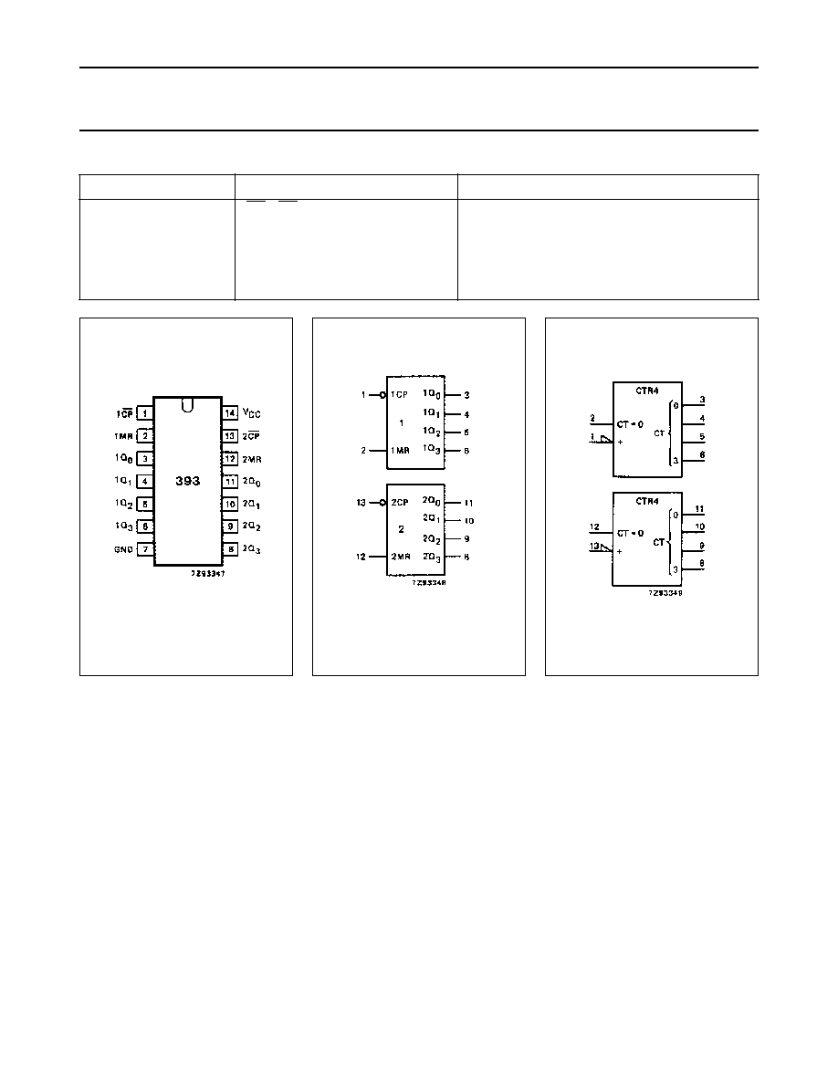
PIN DESCRIPTION
PIN NO.
SYMBOL
NAME AND FUNCTION
1, 13
1CP, 2CP
clock inputs (HIGH-to-LOW, edge-triggered)
2, 12
1MR, 2MR
asynchronous master reset inputs (active HIGH)
3, 4, 5, 6, 11, 10, 9, 8
1Q
0
to 1Q
3
, 2Q
0
to 2Q
3
flip-flop outputs
7
GND
ground (0 V)
14
V
CC
positive supply voltage
Fig.1 Pin configuration.
Fig.2 Logic symbol.
Fig.3 IEC logic symbol.
December 1990
4
Philips Semiconductors
Product specification
Dual 4-bit binary ripple counter
74HC/HCT393
Fig.4 Functional diagram.
Fig.5 State diagram.
Fig.6 Logic diagram (one counter).
COUNT SEQUENCE FOR 1 COUNTER
Notes
1. H = HIGH voltage level
L = LOW voltage level
COUNT
OUTPUTS
Q
0
Q
1
Q
2
Q
3
0
1
2
3
L
H
L
H
L
L
H
H
L
L
L
L
L
L
L
L
4
5
6
7
L
H
L
H
L
L
H
H
H
H
H
H
L
L
L
L
8
9
10
11
L
H
L
H
L
L
H
H
L
L
L
L
H
H
H
H
12
13
14
15
L
H
L
H
L
L
H
H
H
H
H
H
H
H
H
H
December 1990
5
Philips Semiconductors
Product specification
Dual 4-bit binary ripple counter
74HC/HCT393
DC CHARACTERISTICS FOR 74HC
For the DC characteristics see
"74HC/HCT/HCU/HCMOS Logic Family Specifications"
.
Output capability: standard
I
CC
category: MSI
AC CHARACTERISTICS FOR 74HC
GND = 0 V; t
r
= t
f
= 6 ns; C
L
= 50 pF
SYMBOL
PARAMETER
T
amb
(
∞
C)
UNIT
TEST CONDITIONS
74HC
V
CC
(V)
WAVEFORMS
+
25
-
40 to
+
85
-
40 to
+
125
min.
typ. max. min.
max.
min.
max.
t
PHL
/ t
PLH
propagation delay
nCP to nQ
0
41
15
12
125
25
21
155
31
26
190
38
32
ns
2.0
4.5
6.0
Fig.7
t
PHL
/ t
PLH
propagation delay
nQ
n
to nQ
n
+
1
14
5
4
45
9
8
55
11
9
70
14
12
ns
2.0
4.5
6.0
Fig.7
t
PHL
propagation delay
nMR to nQ
n
39
14
11
140
28
24
175
35
30
210
42
36
ns
2.0
4.5
6.0
Fig.8
t
THL
/ t
TLH
output transition time
19
7
6
75
15
13
95
19
16
110
22
19
ns
2.0
4.5
6.0
Fig.7
t
W
clock pulse width
HIGH or LOW
80
16
14
17
6
5
100
20
17
120
24
20
ns
2.0
4.5
6.0
Fig.7
t
W
master reset pulse
width; HIGH
80
16
14
19
7
6
100
20
17
120
24
20
ns
2.0
4.5
6.0
Fig.8
t
rem
removal time
nMR to nCP
5
5
5
3
1
1
5
5
5
5
5
5
ns
2.0
4.5
6.0
Fig.8
f
max
maximum clock pulse
frequency
6
30
35
30
90
107
5
24
28
4
20
24
MHz
2.0
4.5
6.0
Fig.7
December 1990
6
Philips Semiconductors
Product specification
Dual 4-bit binary ripple counter
74HC/HCT393
DC CHARACTERISTICS FOR 74HCT
For the DC characteristics see
"74HC/HCT/HCU/HCMOS Logic Family Specifications"
.
Output capability: standard
I
CC
category: MSI
Note to HCT types
The value of additional quiescent supply current (
I
CC
) for a unit load of 1 is given in the family specifications.
To determine
I
CC
per input, multiply this value by the unit load coefficient shown in the table below.
AC CHARACTERISTICS FOR 74HCT
GND = 0 V; t
r
= t
f
= 6 ns; C
L
= 50 pF
INPUT
UNIT LOAD COEFFICIENT
1CP
2CP
1MR
2MR
0.4
0.4
1.0
1.0
SYMBOL PARAMETER
T
amb
(
∞
C)
UNIT
TEST CONDITIONS
74HCT
V
CC
(V)
WAVEFORMS
+
25
-
40 to
+
85
-
40 to
+
125
min.
typ.
max. min. max. min.
max.
t
PHL
/ t
PLH
propagation delay
nCP to nQ
0
15
25
31
38
ns
4.5
Fig.7
t
PHL
/ t
PLH
propagation delay
nQ
n
to nQ
n
+
1
6
10
13
15
ns
4.5
Fig.7
t
PHL
propagation delay
nMR to nQ
n
18
32
40
48
ns
4.5
Fig.8
t
THL
/ t
TLH
output transition time
7
15
19
22
ns
4.5
Fig.7
t
W
clock pulse width
HIGH or LOW
19
11
24
29
ns
4.5
Fig.7
t
W
master reset pulse
width; HIGH
16
6
20
24
ns
4.5
Fig.8
t
rem
removal time
nMR to nCP
5
0
5
5
ns
4.5
Fig.8
f
max
maximum clock pulse
frequency
27
48
22
18
MHz
4.5
Fig.7
December 1990
7
Philips Semiconductors
Product specification
Dual 4-bit binary ripple counter
74HC/HCT393
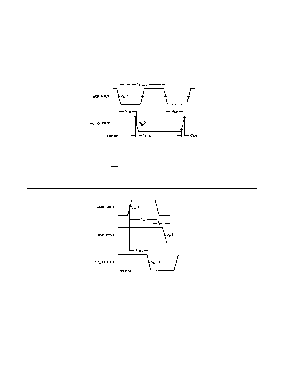
AC WAVEFORMS
PACKAGE OUTLINES
See
"74HC/HCT/HCU/HCMOS Logic Package Outlines"
.
Fig.7
Waveforms showing the clock (nCP) to output (1Q
n
, 2Q
n
) propagation delays, the clock pulse width, the
output transition times and the maximum clock frequency.
(1) HC : V
M
= 50%; V
I
= GND to V
CC
.
HCT: V
M
= 1.3 V; V
I
= GND to 3 V.
Fig.8
Waveforms showing the master reset (nMR) pulse width, the master reset to output (Q
n
) propagation
delays and the master reset to clock (nCP) removal time.
(1) HC : V
M
= 50%; V
I
= GND to V
CC
.
HCT: V
M
= 1.3 V; V
I
= GND to 3 V.