DATA SHEET
Product specification
File under Integrated Circuits, IC06
December 1990
INTEGRATED CIRCUITS
74HC/HCT4002
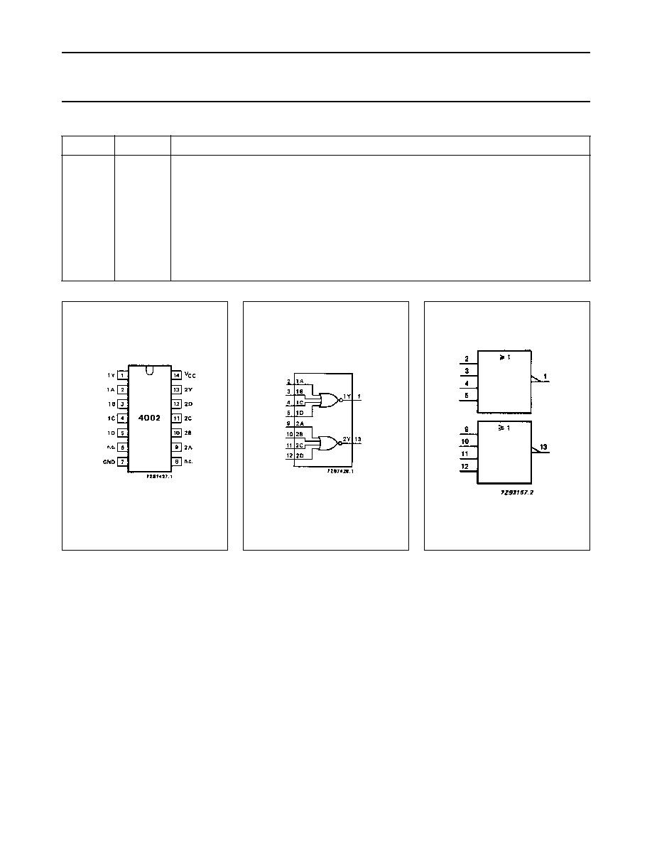
Dual 4-input NOR gate
For a complete data sheet, please also download:
∑
The IC06 74HC/HCT/HCU/HCMOS Logic Family Specifications
∑
The IC06 74HC/HCT/HCU/HCMOS Logic Package Information
∑
The IC06 74HC/HCT/HCU/HCMOS Logic Package Outlines
December 1990
2
Philips Semiconductors
Product specification
Dual 4-input NOR gate
74HC/HCT4002
FEATURES
∑
Output capability: standard
∑
I
CC
category: SSI
GENERAL DESCRIPTION
The 74HC/HCT4002 are high-speed Si-gate CMOS devices and are pin compatible with "4002" of the "4000B" series.
They are specified in compliance with JEDEC standard no. 7A.
The 74HC/HCT4002 provide the 4-input NOR function.
QUICK REFERENCE DATA
GND = 0 V; T
amb
= 25
∞
C; t
r
= t
f
= 6 ns
Notes
1. C
PD
is used to determine the dynamic power dissipation (P
D
in
µ
W):
P
D
= C
PD
◊
V
CC
2
◊
f
i
+
(C
L
◊
V
CC
2
◊
f
o
) where:
f
i
= input frequency in MHz
f
o
= output frequency in MHz
(C
L
◊
V
CC
2
◊
f
o
) = sum of outputs
C
L
= output load capacitance in pF
V
CC
= supply voltage in V
2. For HC the condition is V
I
= GND to V
CC
For HCT the condition is V
I
= GND to V
CC
-
1.5 V
ORDERING INFORMATION
See
"74HC/HCT/HCU/HCMOS Logic Package Information"
.
SYMBOL
PARAMETER
CONDITIONS
TYPICAL
UNIT
HC
HCT
t
PHL
/ t
PLH
propagation delay nA, nB, nC, nD to nY
C
L
= 15 pF; V
CC
= 5 V
9
11
ns
C
I
input capacitance
3.5
3.5
pF
C
PD
power dissipation capacitance per gate
notes 1 and 2
16
22
pF
December 1990
4
Philips Semiconductors
Product specification
Dual 4-input NOR gate
74HC/HCT4002
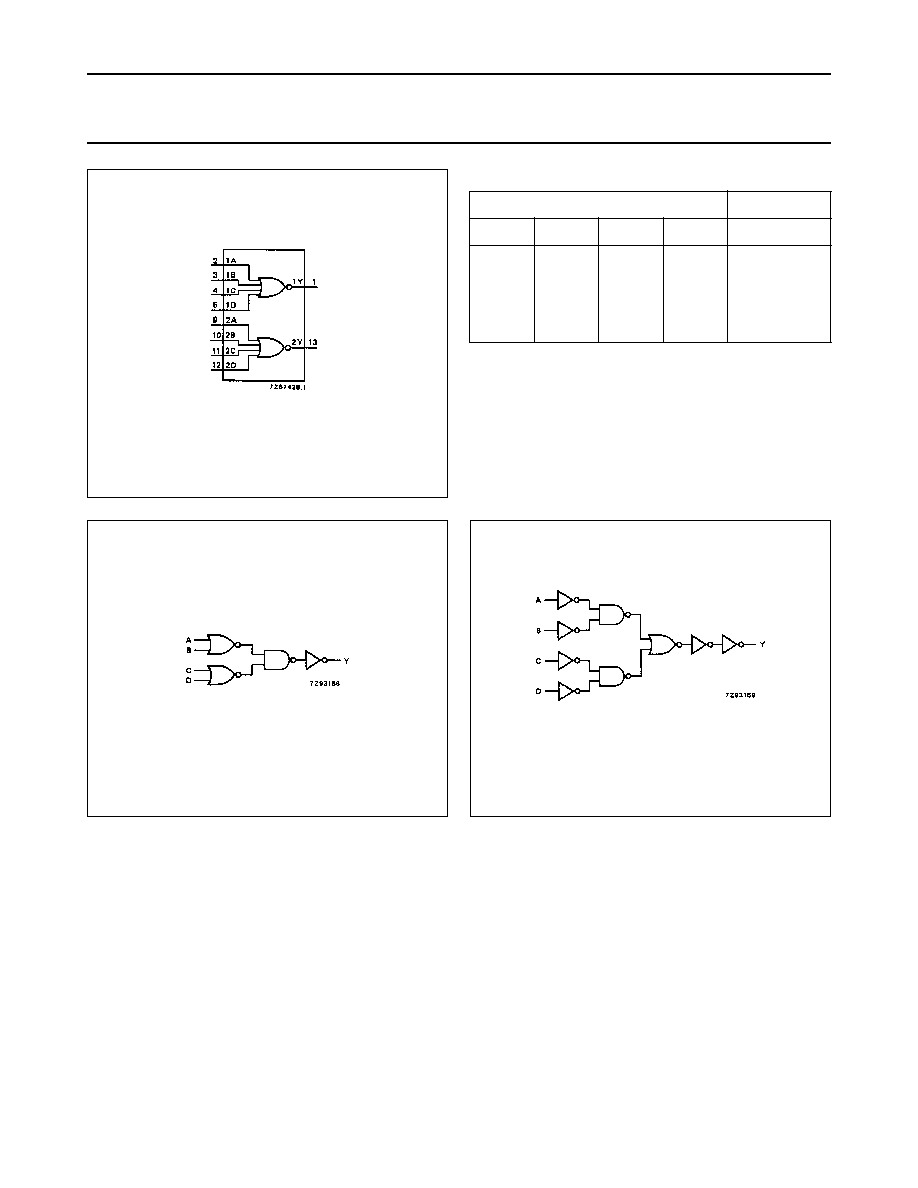
Fig.4 Functional diagram.
FUNCTION TABLE
Notes
1. H = HIGH voltage level
L = LOW voltage level
X = don't care
INPUTS
OUTPUT
nA
nB
nC
nD
nY
L
L
L
L
H
H
X
X
X
X
H
X
X
X
X
H
X
X
X
X
H
L
L
L
L
Fig.5 Logic diagram 74HC4002 (one gate).
Fig.6 Logic diagram 74HCT4002 (one gate).

December 1990
5
Philips Semiconductors
Product specification
Dual 4-input NOR gate
74HC/HCT4002
DC CHARACTERISTICS FOR 74HC
For the DC characteristics see
"74HC/HCT/HCU/HCMOS Logic Family Specifications"
.
Out put capability: standard
I
CC
category: SSI
AC CHARACTERISTICS FOR 74HC
GND = 0 V; t
r
= t
f
= 6 ns; C
L
= 50 pF
SYMBOL PARAMETER
T
amb
(
∞
C)
UNIT
TEST CONDITIONS
74HC
V
CC
(V)
WAVEFORMS
+
25
-
40 to
+
85
-
40 to
+
125
min.
typ.
max.
min.
max.
min.
max.
t
PHL
/ t
PLH
propagation delay
nA, nB, nC, nD to nY
30
11
9
100
20
17
125
25
21
150
30
26
ns
2.0
4.5
6.0
Fig.7
t
THL
/ t
TLH
output transition time
19
7
6
75
15
13
95
19
16
110
22
19
ns
2.0
4.5
6.0
Fig.7