1998 Jan 23
2
Philips Semiconductors
Product specification
4-bit x 16-word FIFO register
74HC/HCT40105
FEATURES
∑
Independent asynchronous inputs and outputs
∑
Expandable in either direction
∑
Reset capability
∑
Status indicators on inputs and outputs
∑
3-state outputs
∑
Output capability: standard
∑
I
CC
category: MSI
GENERAL DESCRIPTION
The 74HC/HCT40105 are high-speed Si-gate CMOS
devices and are pin compatible with the "40105" of the
"4000B" series. They are specified in compliance with
JEDEC standard no. 7A.
The 74HC/HCT40105 are first-in/first-out (FIFO) "elastic"
storage registers that can store sixteen 4-bit words. The
"40105" is capable of handling input and output data at
different shifting rates. This feature makes it particularly
useful as a buffer between asynchronous systems. Each
word position in the register is clocked by a control flip-flop,
which stores a marker bit. A "1" signifies that the position's
data is filled and a "0" denotes a vacancy in that position.
The control flip-flop detects the state of the preceding
flip-flop and communicates its own status to the
succeeding flip-flop. When a control flip-flop is in the "0"
state and sees a "1" in the preceding flip-flop, it generates
a clock pulse that transfers data from the preceding four
data latches into its own four data latches and resets the
preceding flip-flop to "0". The first and last control flip-flops
have buffered outputs. Since all empty locations "bubble"
automatically to the input end, and all valid data ripples
through to the output end, the status of the first control
flip-flop (data-in ready output - DIR) indicates if the FIFO is
full, and the status of the last flip-flop (data-out ready
output - DOR) indicates if the FIFO contains data. As the
earliest data is removed from the bottom of the data stack
(output end), all data entered later will automatically ripple
toward the output.
QUICK REFERENCE DATA
GND = 0 V; T
amb
= 25
∞
C; t
r
= t
f
= 6 ns
Notes
1. C
PD
is used to determine the dynamic power dissipation (P
D
in
µ
W):
P
D
= C
PD
◊
V
CC
2
◊
f
i
+
(C
L
◊
V
CC
2
◊
f
o
) where:
f
i
= input frequency in MHz.
f
o
= output frequency in MHz.
(C
L
◊
V
CC
2
◊
f
o
) = sum of outputs
C
L
= output load capacitance in pF
V
CC
= supply voltage in V
2. For HC the condition is V
I
= GND to V
CC
For HCT the condition is V
I
= GND to V
CC
-
1.5
SYMBOL
PARAMETER
CONDITIONS
TYP.
UNIT
HC
HCT
t
PHL
/ t
PLH
propagation delay
C
L
= 15 pF; V
CC
= 5 V
MR to DIR, DOR
16
15
ns
SO to Q
n
37
35
ns
t
PHL
propagation delay
SI to DIR
16
18
ns
SO to DOR
17
18
ns
f
max
maximum clock frequency
33
31
MHz
C
I
input capacitance
3.5
3.5
pF
C
PD
power dissipation capacitance per package
notes 1 and 2
134
145
pF
1998 Jan 23
3
Philips Semiconductors
Product specification
4-bit x 16-word FIFO register
74HC/HCT40105
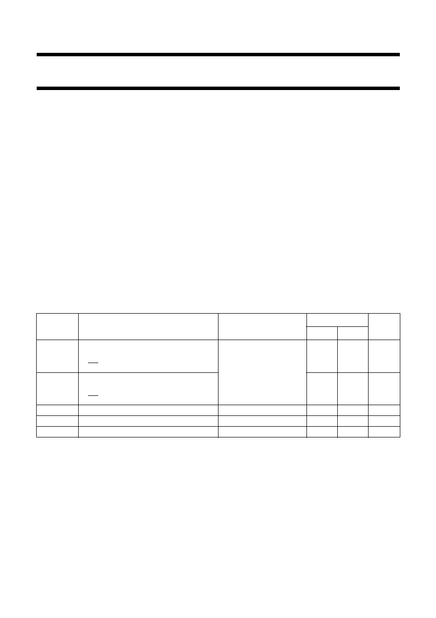
ORDERING INFORMATION
PIN DESCRIPTION
TYPE NUMBER
PACKAGE
NAME
DESCRIPTION
VERSION
74HC(T)40105N
DIP16
plastic dual in-line package; 16 leads (300 mil); long body
SOT38-1
74HC(T)40105D
SO16
plastic small outline package; 16 leads; body width 3.9 mm
SOT109-1
74HC(T)40105DB
SSOP16
plastic shrink small outline package; 16 leads; body width 5.3 mm
SOT338-1
74HC(T)40105PW
TSSOP16
plastic thin shrink small outline package; 16 leads; body width 4.4 mm
SOT403-1
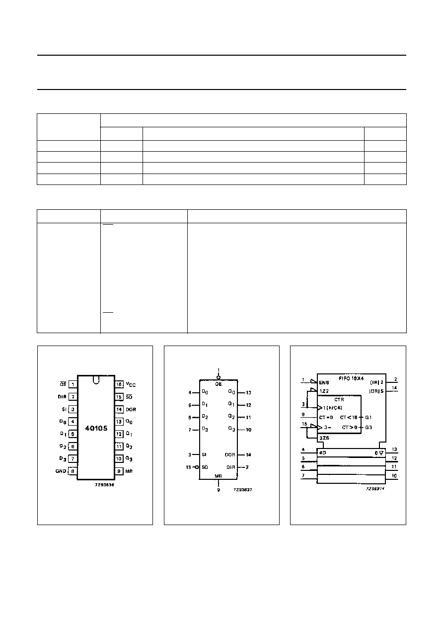
PIN NO.
SYMBOL
NAME AND FUNCTION
1
OE
output enable input (active LOW)
2
DIR
data-in ready output
3
SI
shift-in input (LOW-to-HIGH, edge-triggered)
4, 5, 6, 7
D
0
to D
3
parallel data inputs
8
GND
ground (0 V)
9
MR
asynchronous master reset input (active HIGH)
13, 12, 11, 10
Q
0
to Q
3
3-state data outputs
14
DOR
data-out ready output
15
SO
shift-out input (HIGH-to-LOW, edge-triggered)
16
V
CC
positive supply voltage
Fig.1 Pin configuration.
Fig.2 Logic symbol.
Fig.3 IEC logic symbol.

1998 Jan 23
4
Philips Semiconductors
Product specification
4-bit x 16-word FIFO register
74HC/HCT40105
INPUT AND OUTPUTS
Data inputs (D
0
to D
3
)
As there is no weighting of the inputs,
any input can be assigned as the
MSB. The size of the FIFO memory
can be reduced from the 4
◊
16
configuration, i.e. 3
◊
16, down to
1
◊
16, by tying unused data input
pins to V
CC
or GND.
Data outputs (Q
0
to Q
3
)
As there is no weighting of the
outputs, any output can be assigned
as the MSB. The size of the FIFO
memory can be reduced from the
4
◊
16 configuration as described for
data inputs. In a reduced format, the
unused data outputs pins must be left
open circuit.
Master-reset (MR)
When MR is HIGH, the control
functions within the FIFO are cleared,
and date content is declared invalid.
The data-in ready (DIR) flag is set
HIGH and the data-out-ready (DOR)
flag is set LOW. The output stage
remains in the state of the last word
that was shifted out, or in the random
state existing at power-up.
Status flag outputs (DIR, DOR)
Indication of the status of the FIFO is
given by two status flags,
data-in-ready (DIR) and
data-out-ready (DOR):
DIR = HIGH indicates the input stage
is empty and ready to accept valid
data;
DIR = LOW indicates that the FIFO is
full or that a previous shift-in
operation is not complete (busy);
DOR = HIGH assures valid data is
present at the outputs Q
0
to Q
3
(does
not indicate that new data is awaiting
transfer into the output stage);
DOR = LOW indicates the output
stage is busy or there is no valid data.
Shift-in control (SI)
Data is loaded into the input stage on
a LOW-to-HIGH transition of SI.
It also triggers an automatic data
transfer process (ripple through). If SI
is held HIGH during reset, data will be
loaded at the falling edge of the MR
signal.
Shift-out control (SO)
A HIGH-to-LOW transition of
SO causes the DOR flags to go LOW.
A HIGH-to-LOW transition of
SO causes upstream data to move
into the output stage, and empty
locations to move towards the input
stage (bubble-up).
Output enable (OE)
The outputs Q
0
to Q
3
are enabled
when OE = LOW. When OE = HIGH
the outputs are in the high impedance
OFF-state.
FUNCTIONAL DESCRIPTION
Data input
Following power-up, the master-reset
(MR) input is pulsed HIGH to clear the
FIFO memory (see Fig.8). The
data-in-ready flag (DIR = HIGH)
indicates that the FIFO input stage is
empty and ready to receive data.
When DIR is valid (HIGH), data
present at D
0
to D
3
can be shifted-in
using the SI control input.
With SI = HIGH, data is shifted into
the input stage and a busy indication
is given by DIR going LOW.
The data remains at the first location
in the FIFO until DIR is set to HIGH
and data moves through the FIFO to
the output stage, or to the last empty
location. If the FIFO is not full after the
SI pulse, DIR again becomes valid
(HIGH) to indicate that space is
available in the FIFO. The DIR flag
remains LOW if the FIFO is full (see
Fig.6). The SI use must be made
LOW in order to complete the shift-in
process.
With the FIFO full, SI can be held
HIGH until a shift-out (SO) pulse
occurs. Then, following a shift-out of
data, an empty location appears at
the FIFO input and DIR goes HIGH to
allow the next data to be shifted-in.
This remains at the first FIFO location
until SI goes LOW (see Fig.7).
Data transfer
After data has been transferred from
the input stage of the FIFO following
SI = LOW, data moves through the
FIFO asynchronously and is stacked
at the output end of the register.
Empty locations appear at the input
end of the FIFO as data moves
through the device.
Data output
The data-out-ready flag
(DOR = HIGH) indicates that there is
valid data at the output (Q
0
to Q
3
).
The initial master-reset at power-on
(MR = HIGH) sets DOR to LOW (see
Fig.8). After MR = LOW, data shifted
into the FIFO moves through to the
output stage causing DOR to go
HIGH.
As the DOR flag goes HIGH, data can
be shifted-out using the SO = HIGH,
data in the output stage is shifted out
and a busy indication is given by DOR
going LOW. When SO is made LOW,
data moves through the FIFO to fill
the output stage and an empty
location appears at the input stage.
When the output stage is filled DOR
goes HIGH, but if the last of the valid
data has been shifted-out leaving the
FIFO empty the DOR flag remains
LOW (see Fig.9). With the FIFO
empty, the last word that was
shifted-out is latched at the output
Q
0
to Q
3
.
With the FIFO empty, the SO input
can be held HIGH until the SI control
input is used. Following an SI pulse,

1998 Jan 23
5
Philips Semiconductors
Product specification
4-bit x 16-word FIFO register
74HC/HCT40105
data moves through the FIFO to the
output stage, resulting in the DOR
flag pulsing HIGH and a shift-out of
data occurring. The SO control must
be made LOW before additional data
can be shifted-out (see Fig.10).
High-speed burst mode
If it is assumed that the
shift-in/shift-out pulses are not
applied until the respective status
flags are valid, it follows that the
shift-in/shift-out rates are determined
by the status flags. However, without
the status flags a high-speed burst
mode can be implemented. In this
mode, the burst-in/ burst-out rates are
determined by the pulse widths of the
shift-in/shift-out inputs and burst rates
of 35 MHz can be obtained. Shift
pulses can be applied without regard
to the status flags but shift-in pulses
that would overflow the storage
capacity of the FIFO are not allowed
(see Figs 11 and 12).
Expanded format
With the addition of a logic gate, the
FIFO is easily expanded to increase
word length (see Fig.17). The basic
operation and timing are identical to a
single FIFO, with the exception of an
additional gate delay on the flag
outputs. If during application, the
following occurs:
∑
SI is held HIGH when the FIFO is
empty, some additional logic is
required to produce a composite
DIR pulse (see Figs 7 and 18).
Due to the part-to-part spread of the
ripple through time, the SI signals of
FIFO
A
and FIFO
B
will not always
coincide and the AND-gate will not
produce a composite flag signal. The
solution is given in Fig.18.
The "40105" is easily cascaded to
increase the word capacity and no
external components are needed. In
the cascaded configuration, all
necessary communications and
timing are performed by the FIFOs.
The intercommunication speed is
determined by the minimum flag
pulse widths and the flag delays. The
data rate of cascaded devices is
typically 25 MHz. Word-capacity can
be expanded to and beyond 32-words
◊
4-bits (see Fig.19).