DATA SHEET
Product specification
File under Integrated Circuits, IC06
December 1990
INTEGRATED CIRCUITS
74HC/HCT4017
Johnson decade counter with 10
decoded outputs
For a complete data sheet, please also download:
·
The IC06 74HC/HCT/HCU/HCMOS Logic Family Specifications
·
The IC06 74HC/HCT/HCU/HCMOS Logic Package Information
·
The IC06 74HC/HCT/HCU/HCMOS Logic Package Outlines
December 1990
2
Philips Semiconductors
Product specification
Johnson decade counter with 10 decoded outputs
74HC/HCT4017
FEATURES
·
Output capability: standard
·
I
CC
category: MSI
GENERAL DESCRIPTION
The 74HC/HCT4017 are high-speed Si-gate CMOS
devices and are pin compatible with the "4017" of the
"4000B" series. They are specified in compliance with
JEDEC standard no. 7A.
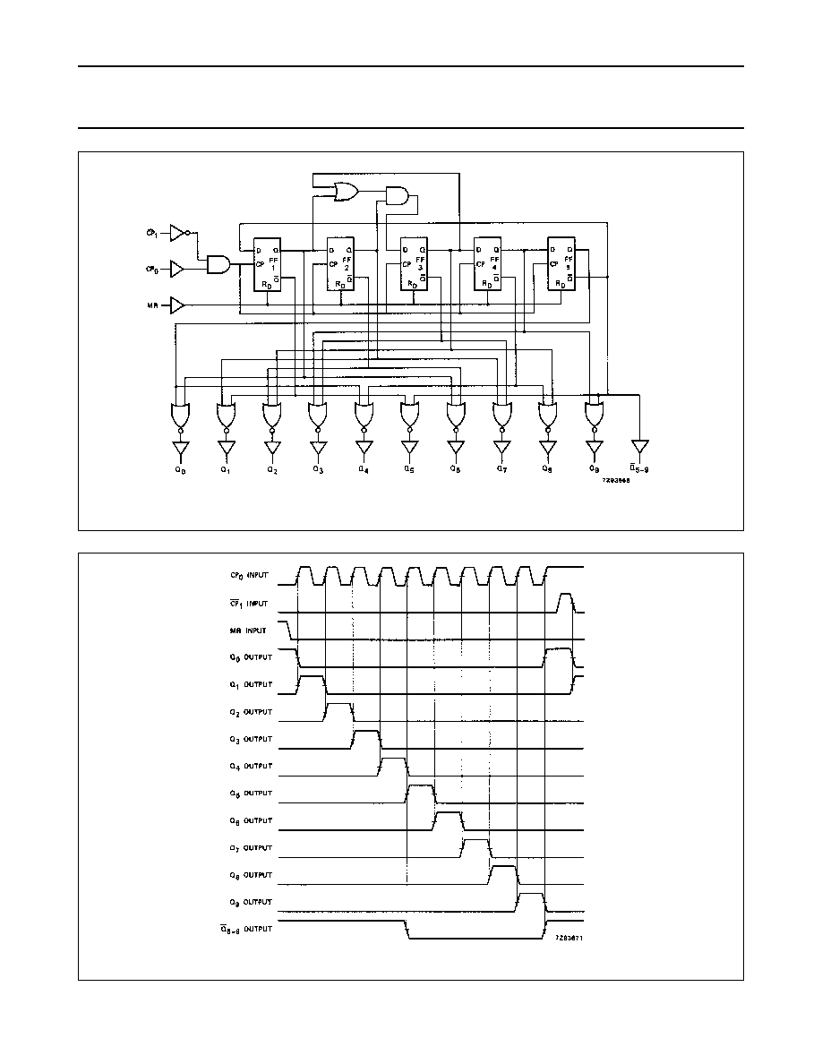
The 74HC/HCT4017 are 5-stage Johnson decade
counters with 10 decoded active HIGH outputs (Q
0
to Q
9
),
an active LOW output from the most significant flip-flop
(Q
5-9
), active HIGH and active LOW clock inputs (CP
0
and
CP
1
) and an overriding asynchronous master reset input
(MR).
The counter is advanced by either a LOW-to-HIGH
transition at CP
0
while CP
1
is LOW or a HIGH-to-LOW
transition at CP
1
while CP
0
is HIGH (see also function
table).
When cascading counters, the Q
5-9
output, which is LOW
while the counter is in states 5, 6, 7, 8 and 9, can be used
to drive the CP
0
input of the next counter.
A HIGH on MR resets the counter to zero
(Q
0
= Q
5-9
= HIGH; Q
1
to Q
9
= LOW) independent of the
clock inputs (CP
0
and CP
1
).
Automatic code correction of the counter is provided by an
internal circuit: following any illegal code the counter
returns to a proper counting mode within 11 clock pulses.
QUICK REFERENCE DATA
GND = 0 V; T
amb
= 25
°
C; t
r
= t
f
= 6 ns
Notes
1. C
PD
is used to determine the dynamic power dissipation (P
D
in
µ
W):
P
D
= C
PD
×
V
CC
2
×
f
i
+
(C
L
×
V
CC
2
×
f
o
) where:
f
i
= input frequency in MHz
f
o
= output frequency in MHz
(C
L
×
V
CC
2
×
f
o
) = sum of outputs
C
L
= output load capacitance in pF
V
CC
= supply voltage in V
2. For HC the condition is V
I
= GND to V
CC
For HCT the condition is V
I
= GND to V
CC
-
1.5 V
ORDERING INFORMATION
See
"74HC/HCT/HCU/HCMOS Logic Package Information"
.
SYMBOL
PARAMETER
CONDITIONS
TYPICAL
UNIT
HC
HCT
t
PHL
/ t
PLH
propagation delay CP
0
, CP
1
to Q
n
C
L
= 15 pF; V
CC
= 5 V 20
21
ns
f
max
maximum clock frequency
77
67
MHz
C
I
input capacitance
3.5
3.5
pF
C
PD
power dissipation capacitance per package
notes 1 and 2
35
36
pF
December 1990
3
Philips Semiconductors
Product specification
Johnson decade counter with 10 decoded outputs
74HC/HCT4017
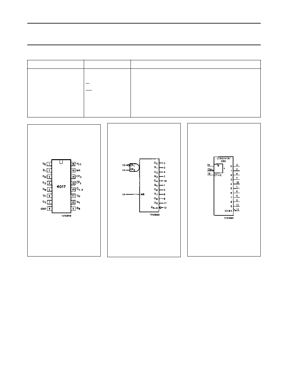
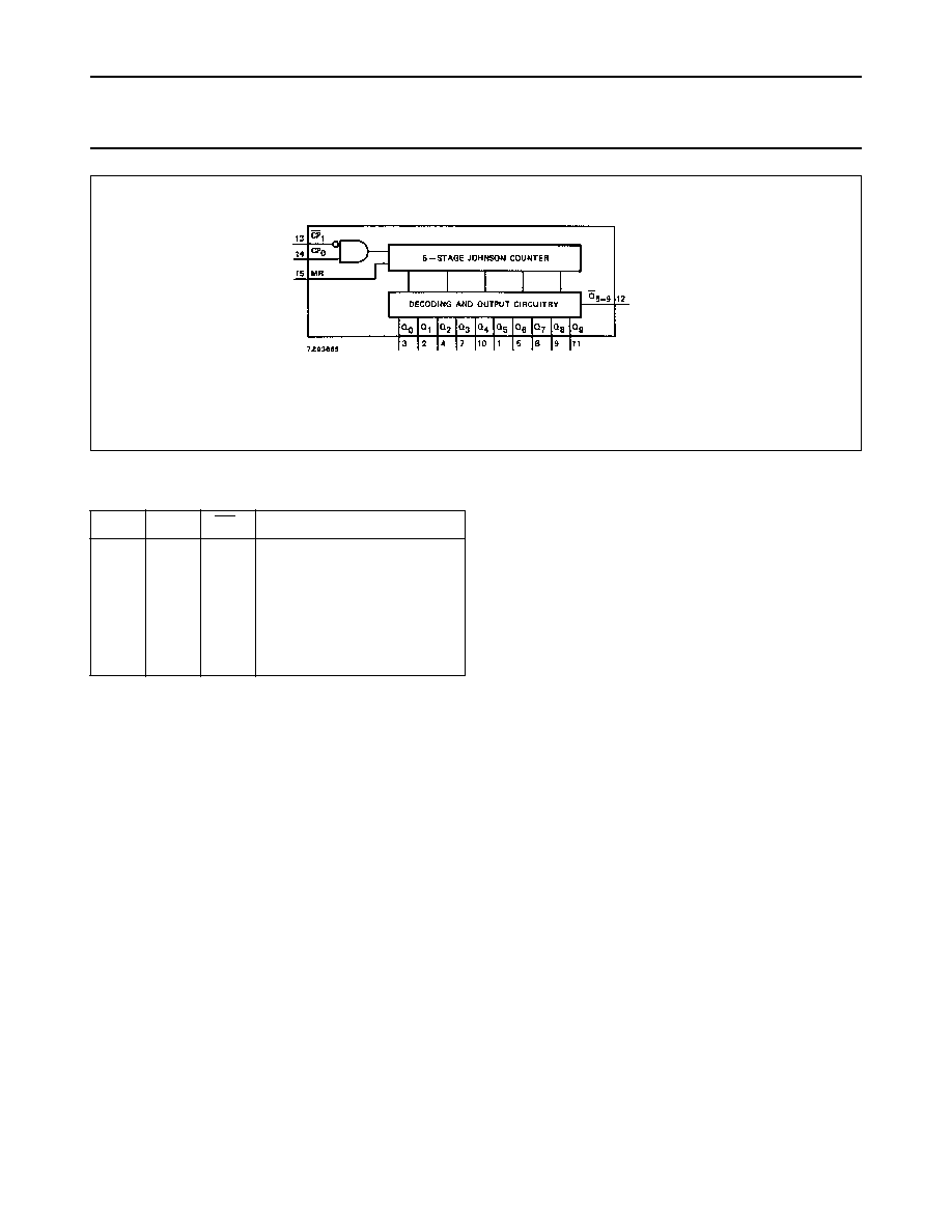
PIN DESCRIPTION
PIN NO.
SYMBOL
NAME AND FUNCTION
3, 2, 4, 7, 10, 1, 5, 6, 9, 11
Q
0
to Q
9
decoded outputs
8
GND
ground (0 V)
12
Q
5-9
carry output (active LOW)
13
CP
1
clock input (HIGH-to-LOW, edge-triggered)
14
CP
0
clock input (LOW-to-HIGH, edge-triggered)
15
MR
master reset input (active HIGH)
16
V
CC
positive supply voltage
Fig.1 Pin configuration.
Fig.2 Logic symbol.
Fig.3 IEC logic symbol.
December 1990
4
Philips Semiconductors
Product specification
Johnson decade counter with 10 decoded outputs
74HC/HCT4017
FUNCTION TABLE
Notes
1. H = HIGH voltage level
L = LOW voltage level
X = don't care
= LOW-to-HIGH clock transition
= HIGH-to-LOW clock transition
MR
CP
0
CP
1
OPERATION
H
X
X
Q
0
= Q
5-9
= H; Q
1
to Q
9
= L
L
L
L
L
L
L
H
L
X
H
L
X
H
L
counter advances
counter advances
no change
no change
no change
no change
Fig.4 Functional diagram.