
DATA SHEET
Product specification
File under Integrated Circuits, IC06
September 1993
INTEGRATED CIRCUITS
74HC/HCT4020
14-stage binary ripple counter
For a complete data sheet, please also download:
∑
The IC06 74HC/HCT/HCU/HCMOS Logic Family Specifications
∑
The IC06 74HC/HCT/HCU/HCMOS Logic Package Information
∑
The IC06 74HC/HCT/HCU/HCMOS Logic Package Outlines
September 1993
2
Philips Semiconductors
Product specification
14-stage binary ripple counter
74HC/HCT4020
FEATURES
∑
Output capability: standard
∑
I
CC
category: MSI
GENERAL DESCRIPTION
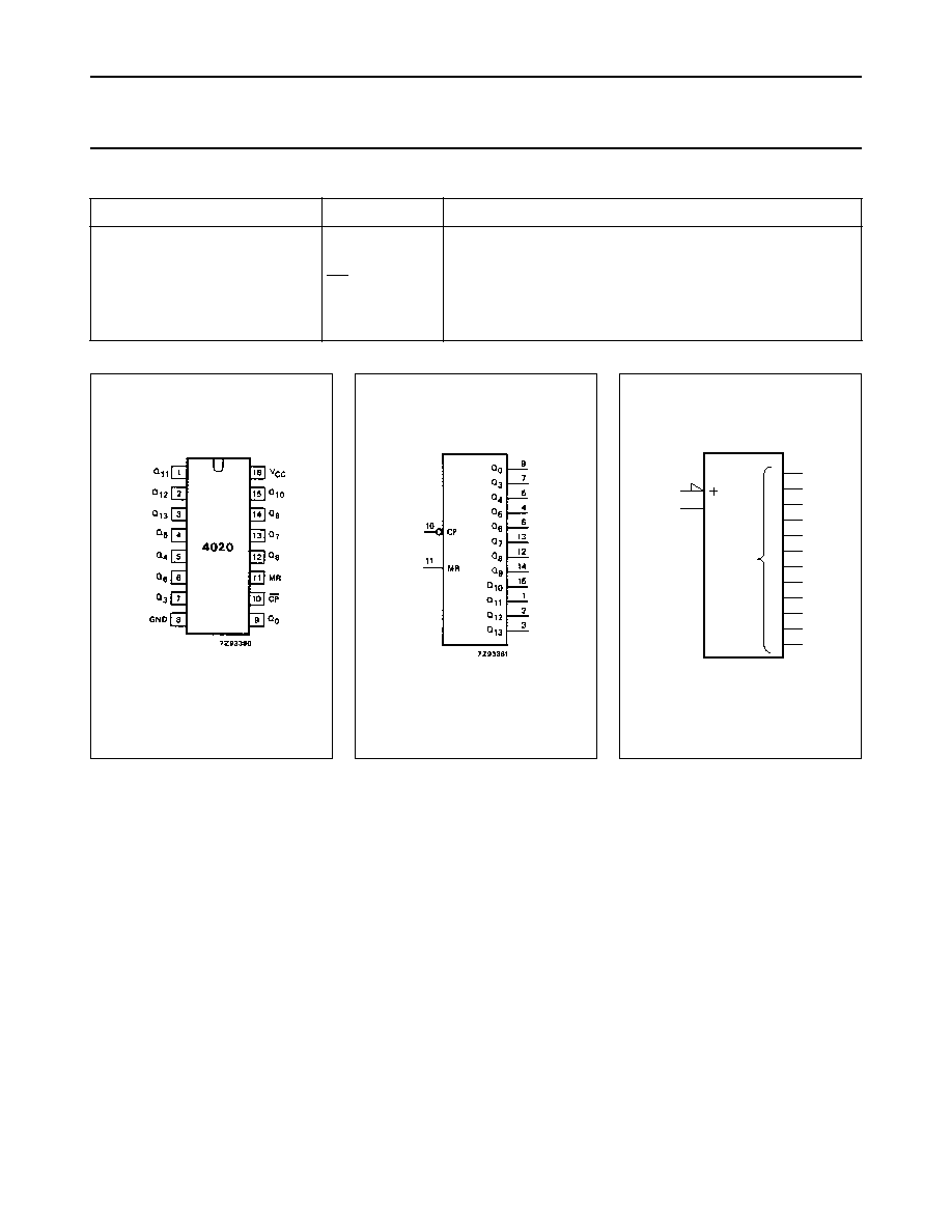
The 74HC/HCT4020 are high-speed Si-gate CMOS
devices and are pin compatible with the "4020" of the
"4000B" series. They are specified in compliance with
JEDEC standard no. 7A.
The 74HC/HCT4020 are 14-stage binary ripple counters
with a clock input (CP), an overriding asynchronous
master reset input (MR) and twelve fully buffered parallel
outputs (Q
0
, Q
3
to Q
13
).
The counter is advanced on the HIGH-to-LOW transition of
CP.
A HIGH on MR clears all counter stages and forces all
outputs LOW, independent of the state of CP.
Each counter stage is a static toggle flip-flop.
QUICK REFERENCE DATA
GND = 0 V; T
amb
= 25
∞
C; t
r
= t
f
= 6 ns
Notes
1. C
PD
is used to determine the dynamic power dissipation (P
D
in
µ
W):
P
D
= C
PD
◊
V
CC
2
◊
f
i
+
(C
L
◊
V
CC
2
◊
f
o
) where:
f
i
= input frequency in MHz
f
o
= output frequency in MHz
(C
L
◊
V
CC
2
◊
f
o
) = sum of outputs
C
L
= output load capacitance in pF
V
CC
= supply voltage in V
2. For HC the condition is V
I
= GND to V
CC
For HCT the condition is V
I
= GND to V
CC
-
1.5 V
ORDERING INFORMATION
See
"74HC/HCT/HCU/HCMOS Logic Package Information"
.
SYMBOL
PARAMETER
CONDITIONS
TYPICAL
UNIT
HC
HCT
t
PHL/
t
PLH
propagation delay
C
L
= 15 pF; V
CC
= 5 V
CP to Q
0
11
15
ns
Q
n
to Q
n
+
1
6
6
ns
MR to Q
n
17
19
ns
f
max
maximum clock frequency
101
52
MHz
C
I
input capacitance
3.5
3.5
pF
C
PD
power dissipation capacitance per package
notes 1 and 2
19
20
pF
September 1993
3
Philips Semiconductors
Product specification
14-stage binary ripple counter
74HC/HCT4020
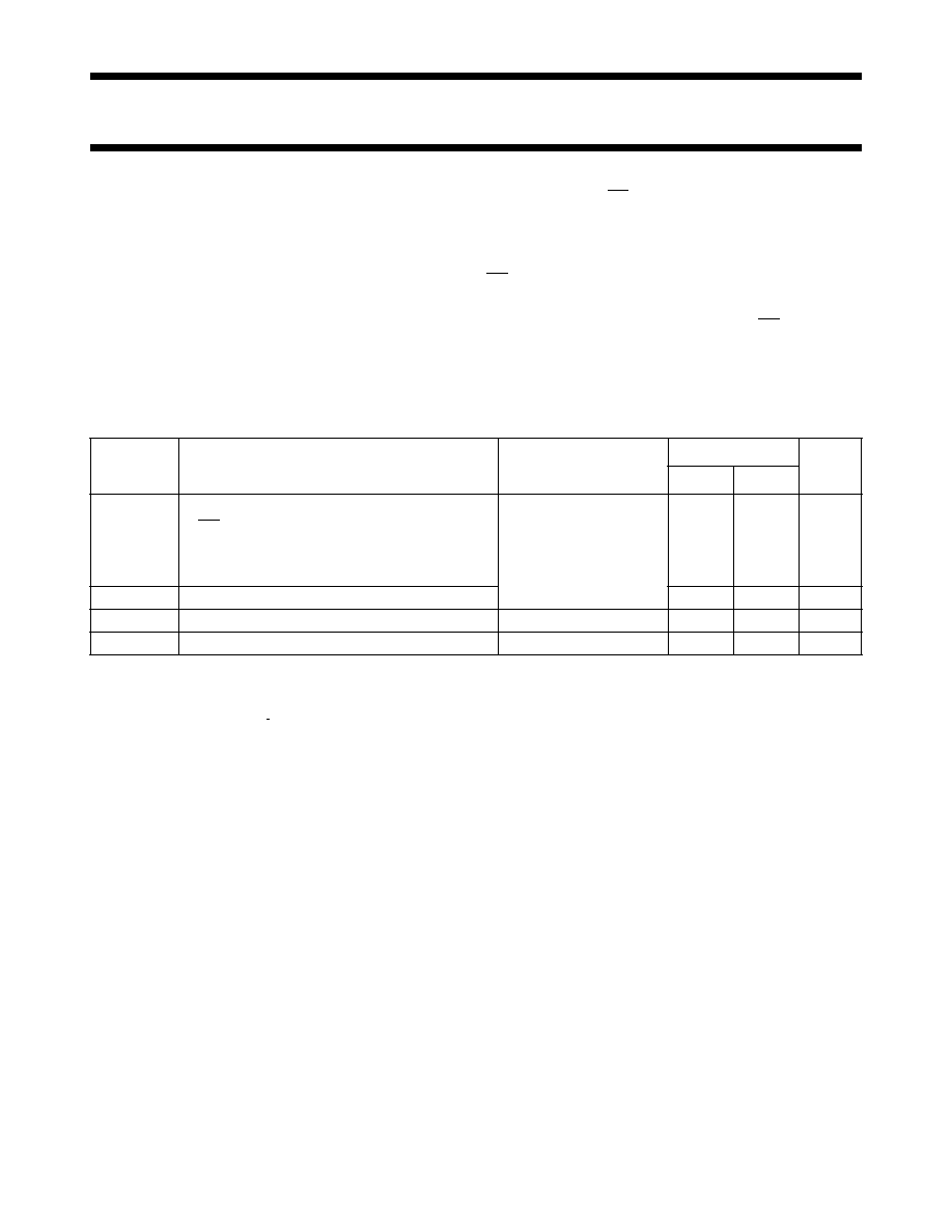
PIN DESCRIPTION
PIN NO.
SYMBOL
NAME AND FUNCTION
9, 7, 5, 4, 6, 13, 12, 14, 15, 1, 2, 3 Q
0
, Q
3
to Q
13
parallel outputs
8
GND
ground (0 V)
10
CP
clock input (HIGH-to-LOW, edge-triggered)
11
MR
master reset input (active HIGH)
16
V
CC
positive supply voltage
Fig.1 Pin configuration.
Fig.2 Logic symbol.
Fig.3 IEC logic symbol.
fpage
MGA829
RCTR14
9
7
5
4
6
13
12
14
15
1
2
3
0
3
13
CT=0
CT
September 1993
4
Philips Semiconductors
Product specification
14-stage binary ripple counter
74HC/HCT4020
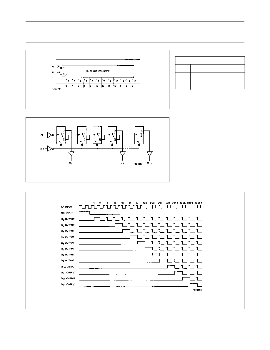
Fig.4 Functional diagram.
Fig.5 Logic diagram.
FUNCTION TABLE
Notes
1. H = HIGH voltage level
L = LOW voltage level
X = don't care
= LOW-to-HIGH clock
transition
= HIGH-to-LOW clock
transition
INPUTS
OUTPUTS
CP
MR
Q
0
, Q
3
to Q
13
X
L
L
H
no change
count
L
Fig.6 Timing diagram.

September 1993
5
Philips Semiconductors
Product specification
14-stage binary ripple counter
74HC/HCT4020
DC CHARACTERISTICS FOR 74HC
For the DC characteristics see
"74HC/HCT/HCU/HCMOS Logic Family Specifications"
.
Output capability: standard
I
CC
category: MSI
AC CHARACTERISTICS FOR 74HC
GND = 0 V; t
r
= t
f
= 6 ns; C
L
= 50 pF
SYMBOL
PARAMETER
T
amb
(
∞
C)
UNIT
TEST CONDITIONS
74HC
V
CC
(V)
WAVEFORMS
+
25
-
40 to
+
85
-
40 to
+
125
min.
typ.
max.
min.
max.
min.
max.
t
PHL
/ t
PLH
propagation delay
CP to Q
0
39
14
11
140
28
24
175
35
30
210
42
36
ns
2.0
4.5
6.0
Fig.7
t
PHL
/ t
PLH
propagation delay
Q
n
to Q
n
+
1
22
8
6
75
15
13
95
19
16
110
22
19
ns
2.0
4.5
6.0
Fig.7
t
PHL
propagation delay
MR to Q
n
55
20
16
170
34
29
215
43
37
225
51
43
ns
2.0
4.5
6.0
Fig.8
t
THL
/ t
TLH
output transition time
19
7
6
75
15
13
95
19
16
110
22
19
ns
2.0
4.5
6.0
Fig.7
t
W
clock pulse width
HIGH or LOW
80
16
14
11
4
3
100
20
17
120
24
20
ns
2.0
4.5
6.0
Fig.7
t
W
master reset pulse width
HIGH
80
16
14
17
6
5
100
20
17
120
24
20
ns
2.0
4.5
6.0
Fig.8
t
rem
removal time
MR to CP
50
10
9
6
2
2
65
13
11
75
15
13
ns
2.0
4.5
6.0
Fig.8
f
max
maximum clock pulse
frequency
6.0
30
35
30
92
109
4.8
24
28
4.0
20
24
MHz
2.0
4.5
6.0
Fig.7