 | –≠–ª–µ–∫—Ç—Ä–æ–Ω–Ω—ã–π –∫–æ–º–ø–æ–Ω–µ–Ω—Ç: 74HC4024N | –°–∫–∞—á–∞—Ç—å:  PDF PDF  ZIP ZIP |

1.
General description
The 74HC4024 is a high-speed Si-gate CMOS device and is pin compatible with the 4024
of the 4000B series. The 74HC4024 is specified in compliance with JEDEC
standard no. 7A.
The 74HC4024 is a 7-stage binary ripple counter with a clock input (CP), an overriding
asynchronous master reset input (MR) and seven fully buffered parallel outputs (Q0 to
Q6).
The counter advances on the HIGH-to-LOW transition of CP.
A HIGH on MR clears all counter stages and forces all outputs LOW, independent of the
state of CP.
Each counter stage is a static toggle flip-flop.
Schmitt-trigger action in the clock input makes the circuit highly tolerant to slower clock
rise and fall times.
2.
Features
s
Low-power dissipation
s
Complies with JEDEC standard no. 7A
s
ESD protection:
x
HBM EIA/JESD22-A114-B exceeds 2000 V
x
MM EIA/JESD22-A115-A exceeds 200 V.
s
Multiple package options
s
Specified from
-
40
∞
C to +80
∞
C and from
-
40
∞
C to +125
∞
C.
3.
Applications
s
Frequency dividing circuits
s
Time delay circuits.
74HC4024
7-stage binary ripple counter
Rev. 03 -- 12 November 2004
Product data sheet
9397 750 13813
© Koninklijke Philips Electronics N.V. 2004. All rights reserved.
Product data sheet
Rev. 03 -- 12 November 2004
2 of 18
Philips Semiconductors
74HC4024
7-stage binary ripple counter
4.
Quick reference data
[1]
C
PD
is used to determine the dynamic power dissipation (P
D
in
µ
W).
P
D
= C
PD
◊
V
CC
2
◊
f
i
◊
N +
(C
L
◊
V
CC
2
◊
f
o
) where:
f
i
= input frequency in MHz;
f
o
= output frequency in MHz;
C
L
= output load capacitance in pF;
V
CC
= supply voltage in V;
N = number of inputs switching;
(C
L
◊
V
CC
2
◊
f
o
) = sum of outputs.
5.
Ordering information
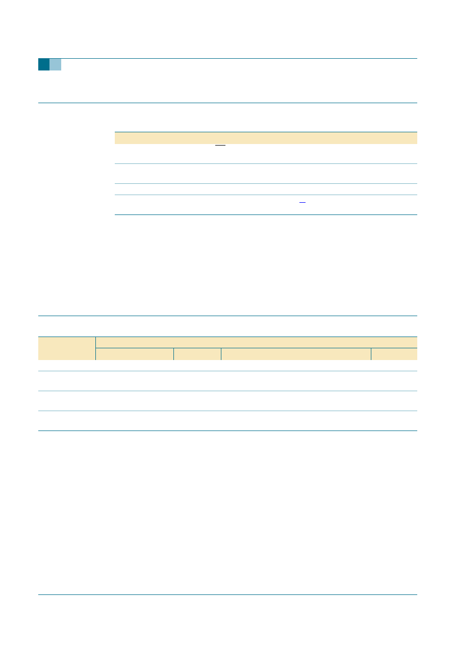
Table 1:
Quick reference data
GND = 0 V; T
amb
= 25
∞
C; t
r
= t
f
= 6 ns.
Symbol
Parameter
Conditions
Min
Typ
Max
Unit
t
PHL
, t
PLH
propagation delay CP to
Q0
C
L
= 15 pF;
V
CC
= 5 V
-
14
-
ns
f
max
maximum clock frequency C
L
= 15 pF;
V
CC
= 5 V
-
90
-
MHz
C
I
input capacitance
-
3.5
-
pF
C
PD
power dissipation
capacitance
V
I
= GND to V
CC
[1]
-
25
-
pF
Table 2:
Ordering information
Type number
Package
Temperature range
Name
Description
Version
74HC4024N
-
40
∞
C to +125
∞
C
DIP14
plastic dual in-line package; 14 leads (300 mil)
SOT27-1
74HC4024D
-
40
∞
C to +125
∞
C
SO14
plastic small outline package; 14 leads;
body width 3.9 mm
SOT108-1
74HC4024DB
-
40
∞
C to +125
∞
C
SSOP14
plastic shrink small outline package; 14 leads;
body width 5.3 mm
SOT337-1
74HC4024PW
-
40
∞
C to +125
∞
C
TSSOP14
plastic thin shrink small outline package;
14 leads; body width 4.4 mm
SOT402-1

9397 750 13813
© Koninklijke Philips Electronics N.V. 2004. All rights reserved.
Product data sheet
Rev. 03 -- 12 November 2004
3 of 18
Philips Semiconductors
74HC4024
7-stage binary ripple counter
6.
Functional diagram
Fig 1.
Functional diagram
Fig 2.
Logic symbol
Fig 3.
IEC logic symbol
001aab908
MR
Q3
Q4
Q5
Q6
6
5
4
3
7-STAGE
COUNTER
Q0
Q1
Q2
12
11
9
2
CP
1
001aab906
MR
2
Q0
Q1
Q2
Q3
Q4
Q5
Q6
3
4
5
6
9
11
12
CP
1
001aab907
CT = 0
CT
2
0
6
3
4
5
6
9
11
12
CTR7
+
1
Fig 4.
Logic diagram
001aab909
RD
FF
1
T
CP
Q
Q
MR
RD
FF
2
T
Q
Q
RD
FF
3
T
Q
Q
RD
FF
4
T
Q
Q
RD
FF
5
T
Q
Q
RD
FF
6
T
Q
Q
RD
Q0
Q1
Q2
Q3
Q4
Q5
Q6
FF
7
T
Q
Q

9397 750 13813
© Koninklijke Philips Electronics N.V. 2004. All rights reserved.
Product data sheet
Rev. 03 -- 12 November 2004
4 of 18
Philips Semiconductors
74HC4024
7-stage binary ripple counter
7.
Pinning information
7.1 Pinning
7.2 Pin description
Fig 5.
Pin configuration
4024
CP
V
CC
MR
n.c.
Q6
Q0
Q5
Q1
Q4
n.c.
Q3
Q2
GND
n.c.
001aab905
1
2
3
4
5
6
7
8
10
9
12
11
14
13
Table 3:
Pin description
Symbol
Pin
Description
CP
1
clock input (HIGH-to-LOW, edge-triggered)
MR
2
master reset input (active HIGH)
Q6
3
parallel output 6
Q5
4
parallel output 5
Q4
5
parallel output 4
Q3
6
parallel output 3
GND
7
ground (0 V)
n.c.
8
not connected
Q2
9
parallel output 2
n.c.
10
not connected
Q1
11
parallel output 1
Q0
12
parallel output 0
n.c.
13
not connected
V
CC
14
positive supply voltage

9397 750 13813
© Koninklijke Philips Electronics N.V. 2004. All rights reserved.
Product data sheet
Rev. 03 -- 12 November 2004
5 of 18
Philips Semiconductors
74HC4024
7-stage binary ripple counter
8.
Functional description
8.1 Function table
[1]
H = HIGH voltage level;
L = LOW voltage level;
X = don't care;
= LOW-to-HIGH clock transition;
=
HIGH-to-LOW clock transition.
9.
Limiting values
[1]
Above 70
∞
C: P
tot
derates linearly with 12 mW/K.
[2]
Above 70
∞
C: P
tot
derates linearly with 8 mW/K.
Table 4:
Function table
[1]
Input
Output
MR
CP
Qn
H
X
L
L
no change
count
Table 5:
Limiting values
In accordance with the Absolute Maximum Rating System (IEC 60134). Voltages are referenced to
GND (ground = 0 V).
Symbol
Parameter
Conditions
Min
Max
Unit
V
CC
supply voltage
-
0.5
+7
V
I
IK
input diode current
V
I
<
-
0.5 V or V
I
> V
CC
+ 0.5 V
-
±
20
mA
I
OK
output diode current
V
O
<
-
0.5 V or
V
O
> V
CC
+ 0.5 V
-
±
20
mA
I
O
output source or sink
current
V
O
=
-
0.5 V to V
CC
+ 0.5 V
-
±
25
mA
I
CC
, I
GND
V
CC
or GND current
-
±
50
mA
T
stg
storage temperature
-
65
+150
∞
C
P
tot
power dissipation
DIP14 package
[1]
-
750
mW
SO14, SSOP14 and
TSSOP14 packages
[2]
-
500
mW