
1.
General description
The 74HC4040; 74HCT4040 are high-speed Si-gate CMOS devices and are pin
compatible with the HEF4040B series. They are specified in compliance with JEDEC
standard no. 7A.
The 74HC4040; 74HCT4040 are 12-stage binary ripple counters with a clock input (CP),
an overriding asynchronous master reset input (MR) and twelve parallel outputs (Q0 to
Q11). The counter advances on the HIGH-to-LOW transition of CP.
A HIGH on MR clears all counter stages and forces all outputs LOW, independent of the
state of CP.
Each counter stage is a static toggle flip-flop.
2.
Features
s
Multiple package options
s
Complies with JEDEC standard no. 7A
s
ESD protection:
x
HBM JESD22-A114-C exceeds 2000 V
x
MM JESD22-A115-A exceeds 200 V
s
Specified from
-
40
�
C to +85
�
C and from
-
40
�
C to +125
�
C
3.
Applications
s
Frequency dividing circuits
s
Time delay circuits
s
Control counters
4.
Quick reference data
74HC4040; 74HCT4040
12-stage binary ripple counter
Rev. 03 -- 14 September 2005
Product data sheet
Table 1:
Quick reference data
GND = 0 V; T
amb
= 25
�
C; t
r
= t
f
= 6 ns.
Symbol
Parameter
Conditions
Min
Typ
Max
Unit
Type 74HC4040
t
PHL
, t
PLH
propagation delay
CP to Q0
C
L
= 15 pF; V
CC
= 5 V
-
14
-
ns
Qn to Qn+1
C
L
= 15 pF; V
CC
= 5 V
-
8
-
ns
74HC_HCT4040_3
� Koninklijke Philips Electronics N.V. 2005. All rights reserved.
Product data sheet
Rev. 03 -- 14 September 2005
2 of 24
Philips Semiconductors
74HC4040; 74HCT4040
12-stage binary ripple counter
[1]
C
PD
is used to determine the dynamic power dissipation (P
D
in
�
W):
P
D
= C
PD
�
V
CC
2
�
f
i
+
(C
L
�
V
CC
2
�
f
o
) where:
f
i
= input frequency in MHz;
f
o
= output frequency in MHz;
(C
L
�
V
CC
2
�
f
o
) = sum of outputs;
C
L
= output load capacitance in pF;
V
CC
= supply voltage in V.
5.
Ordering information
f
max
maximum operating
frequency
C
L
= 15 pF; V
CC
= 5 V
-
90
-
MHz
C
i
input capacitance
-
3.5
-
pF
C
PD
power dissipation
capacitance
V
I
= GND to V
CC
-
20
-
pF
Type 74HCT4040
t
PHL
, t
PLH
propagation delay
CP to Q0
C
L
= 15 pF; V
CC
= 5 V
-
16
-
ns
Qn to Qn+1
C
L
= 15 pF; V
CC
= 5 V
-
8
-
ns
f
max
maximum operating
frequency
C
L
= 15 pF; V
CC
= 5 V
-
79
-
MHz
C
i
input capacitance
-
3.5
-
pF
C
PD
power dissipation
capacitance
V
I
= GND to V
CC
-
1.5 V
-
20
-
pF
Table 1:
Quick reference data
...continued
GND = 0 V; T
amb
= 25
�
C; t
r
= t
f
= 6 ns.
Symbol
Parameter
Conditions
Min
Typ
Max
Unit
Table 2:
Ordering information
Type number
Package
Temperature range
Name
Description
Version
74HC4040N
-
40
�
C to +125
�
C
DIP16
plastic dual in-line package; 16 leads (300 mil);
long body
SOT38-1
74HC4040D
-
40
�
C to +125
�
C
SO16
plastic small outline package; 16 leads; body
width 3.9 mm
SOT109-1
74HC4040DB
-
40
�
C to +125
�
C
SSOP16
plastic shrink small outline package; 16 leads; body
width 5.3 mm
SOT338-1
74HC4040PW
-
40
�
C to +125
�
C
TSSOP16
plastic thin shrink small outline package; 16 leads;
body width 4.4 mm
SOT403-1
74HC4040BQ
-
40
�
C to +125
�
C
DHVQFN16 plastic dual in-line compatible thermal enhanced
very thin quad flat package; no leads; 16 terminals;
body 2.5
�
3.5
�
0.85 mm
SOT763-1
74HCT4040N
-
40
�
C to +125
�
C
DIP16
plastic dual in-line package; 16 leads (300 mil);
long body
SOT38-1
74HCT4040D
-
40
�
C to +125
�
C
SO16
plastic small outline package; 16 leads; body
width 3.9 mm
SOT109-1
74HC_HCT4040_3
� Koninklijke Philips Electronics N.V. 2005. All rights reserved.
Product data sheet
Rev. 03 -- 14 September 2005
3 of 24
Philips Semiconductors
74HC4040; 74HCT4040
12-stage binary ripple counter
6.
Functional diagram
74HCT4040DB
-
40
�
C to +125
�
C
SSOP16
plastic shrink small outline package; 16 leads; body
width 5.3 mm
SOT338-1
74HCT4040PW
-
40
�
C to +125
�
C
TSSOP16
plastic thin shrink small outline package; 16 leads;
body width 4.4 mm
SOT403-1
74HCT4040BQ
-
40
�
C to +125
�
C
DHVQFN16 plastic dual in-line compatible thermal enhanced
very thin quad flat package; no leads; 16 terminals;
body 2.5
�
3.5
�
0.85 mm
SOT763-1
Table 2:
Ordering information
...continued
Type number
Package
Temperature range
Name
Description
Version
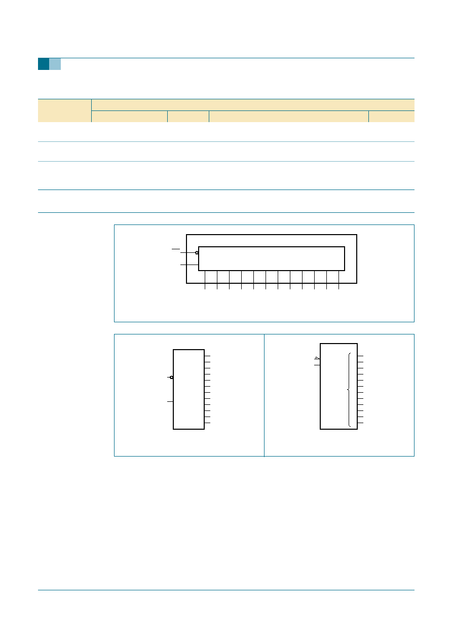
Fig 1.
Functional diagram
Fig 2.
Logic symbol
Fig 3.
IEC logic symbol
001aad589
12-STAGE COUNTER
9
Q0
7
Q1
6
Q2
5
Q3
3
Q4
2
Q5
4
Q6
13
Q7
12
Q8
14
Q9
15
Q10
1
Q11
10
11
T
C
D
MR
CP
001aad585
Q0
9
11
MR
10
CP
Q1
7
Q2
6
Q3
5
Q4
3
Q5
2
Q6
4
Q7
13
Q8
12
Q9
14
Q10
15
Q11
1
001aad586
0
9
11
CT = 0
+
10
CTR12
CT
7
6
5
3
2
4
13
12
14
15
11
1
74HC_HCT4040_3
� Koninklijke Philips Electronics N.V. 2005. All rights reserved.
Product data sheet
Rev. 03 -- 14 September 2005
4 of 24
Philips Semiconductors
74HC4040; 74HCT4040
12-stage binary ripple counter
7.
Pinning information
7.1 Pinning
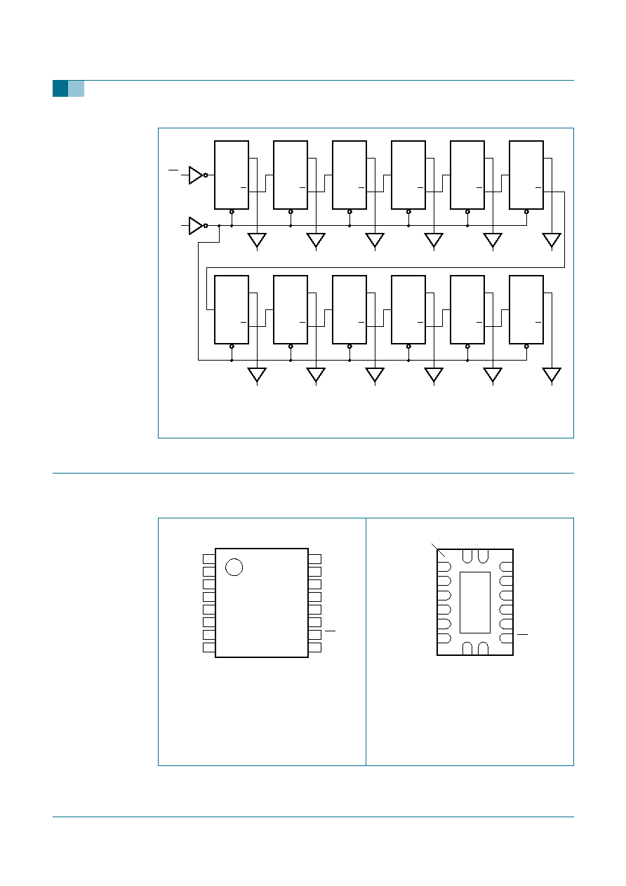
Fig 4.
Logic diagram
001aad588
CP
MR
FF
1
Q
T
RD
Q0
Q
FF
2
Q
T
RD
Q1
Q
FF
7
Q
T
RD
Q6
Q
FF
8
Q
T
RD
Q7
Q
FF
9
Q
T
RD
Q8
Q
FF
10
Q
T
RD
Q9
Q
FF
11
Q
T
RD
Q10
Q
FF
12
Q
T
RD
Q11
Q
FF
3
Q
T
RD
Q2
Q
FF
4
Q
T
RD
Q3
Q
FF
5
Q
T
RD
Q4
Q
FF
6
Q
T
RD
Q5
Q
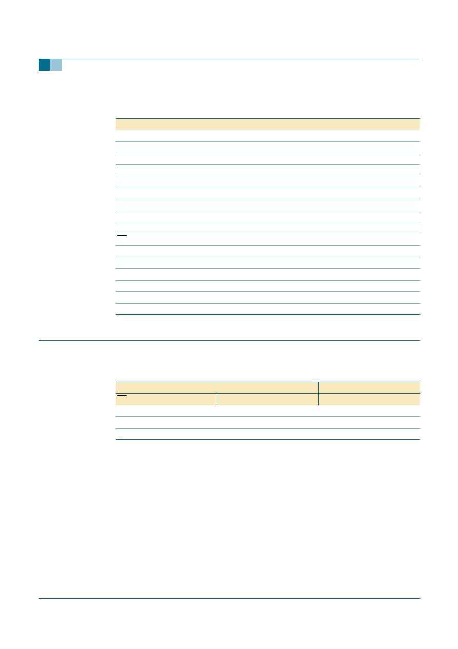
(1) The substrate is attached to this pad
using conductive die attach material. It
can not be used as supply pin or input
Fig 5.
Pin configuration DIP16, SO16,
SSOP16 and TSSOP16
Fig 6.
Pin configuration DHVQFN16
4040
Q11
V
CC
Q5
Q10
Q4
Q9
Q6
Q7
Q3
Q8
Q2
MR
Q1
CP
GND
Q0
001aad583
1
2
3
4
5
6
7
8
10
9
12
11
14
13
16
15
001aad584
4040
Q1
CP
Q2
MR
Q3
Q8
Q6
Q7
Q4
Q9
Q5
Q10
GND
Q0
Q11
V
CC
Transparent top view
7
10
6
11
5
12
4
13
3
14
2
15
8
9
1
16
terminal 1
index area
GND
(1)
74HC_HCT4040_3
� Koninklijke Philips Electronics N.V. 2005. All rights reserved.
Product data sheet
Rev. 03 -- 14 September 2005
5 of 24
Philips Semiconductors
74HC4040; 74HCT4040
12-stage binary ripple counter
7.2 Pin description
8.
Functional description
8.1 Function table
[1]
H = HIGH voltage level;
L = LOW voltage level;
X = don't care;
= LOW-to-HIGH clock transition;
= HIGH-to-LOW clock transition.
Table 3:
Pin description
Symbol
Pin
Description
Q11
1
output 11
Q5
2
output 5
Q4
3
output 4
Q6
4
output 6
Q3
5
output 3
Q2
6
output 2
Q1
7
output 1
GND
8
ground (0 V)
Q0
9
output 0
CP
10
clock input (HIGH-to-LOW, edge-triggered)
MR
11
master reset input (active HIGH)
Q8
12
output 8
Q7
13
output 7
Q9
14
output 9
Q10
15
output 10
V
CC
16
positive supply voltage
Table 4:
Function table
Input
Output
CP
MR
Q0 to Q11
L
no change
L
count
X
H
L