 | –≠–ª–µ–∫—Ç—Ä–æ–Ω–Ω—ã–π –∫–æ–º–ø–æ–Ω–µ–Ω—Ç: 74HC4052U | –°–∫–∞—á–∞—Ç—å:  PDF PDF  ZIP ZIP |
Document Outline
- FEATURES
- APPLICATIONS
- DESCRIPTION
- FUNCTION TABLE
- QUICK REFERENCE DATA
- ORDERING INFORMATION
- PINNING
- LIMITING VALUES
- RECOMMENDED OPERATING CONDITIONS
- DC CHARACTERISTICS
- AC CHARACTERISTICS
- AC WAVEFORMS
- PACKAGE OUTLINES
- SOT109-3
- SOT338-1
- SOT38-9
- SOT403-1
- SOT763-1
- SOLDERING
- DATA SHEET STATUS
- DEFINITIONS
- DISCLAIMERS

DATA SHEET
Product specification
Supersedes data of 1997 Aug 27
2003 May 16
INTEGRATED CIRCUITS
74HC4052; 74HCT4052
Dual 4-channel analog multiplexer,
demultiplexer

2003 May 16
2
Philips Semiconductors
Product specification
Dual 4-channel analog multiplexer,
demultiplexer
74HC4052; 74HCT4052
FEATURES
∑
Wide analog input voltage range from
-
5 V to +5 V
∑
Low ON-resistance:
≠ 80
(typical) at V
CC
-
V
EE
= 4.5 V
≠ 70
(typical) at V
CC
-
V
EE
= 6.0 V
≠ 60
(typical) at V
CC
-
V
EE
= 9.0 V
∑
Logic level translation: to enable 5 V logic to
communicate with
±
5 V analog signals
∑
Typical "break before make" built in
∑
Complies with JEDEC standard no. 8-1 A
∑
ESD protection:
≠ HBM EIA/JESD22-A114-A exceeds 2000 V
≠ MM EIA/JESD22-A115-A exceeds 200 V.
∑
Specified from
-
40 to +85
∞
C and
-
40 to +125
∞
C.
APPLICATIONS
∑
Analog multiplexing and demultiplexing
∑
Digital multiplexing and demultiplexing
∑
Signal gating.
DESCRIPTION
The 74HC4052/74HCT4052 are high-speed Si-gate
CMOS devices and are pin compatible with the
HEF4052B. They are specified in compliance with JEDEC
standard no. 7A.
The 74HC4052/74HCT4052 are dual 4-channel analog
multiplexers or demultiplexers with common select logic.
Each multiplexer has four independent inputs/outputs
(pins nY0 to nY3) and a common input/output (pin nZ). The
common channel select logics include two digital select
inputs (pins S0 and S1) and an active LOW enable input
(pin E). When pin E = LOW, one of the four switches is
selected (low-impedance ON-state) with pins S0 and S1.
When pin E = HIGH, all switches are in the
high-impedance OFF-state, independent of pins S0 and
S1.
V
CC
and GND are the supply voltage pins for the digital
control inputs (pins S0, S1, and E). The V
CC
to GND
ranges are 2.0 to 10.0 V for 74HC4052 and 4.5 to 5.5 V
for 74HCT4052. The analog inputs/outputs (pins nY0 to
nY3 and nZ) can swing between V
CC
as a positive limit and
V
EE
as a negative limit. V
CC
-
V
EE
may not exceed 10.0 V.
For operation as a digital multiplexer/demultiplexer, V
EE
is
connected to GND (typically ground).
FUNCTION TABLE
Note
1. H = HIGH voltage level
L = LOW voltage level
X = don't care.
INPUT
(1)
CHANNEL BETWEEN
E
S1
S0
L
L
L
nY0 and nZ
L
L
H
nY1 and nZ
L
H
L
nY2 and nZ
L
H
H
nY3 and nZ
H
X
X
none
2003 May 16
3
Philips Semiconductors
Product specification
Dual 4-channel analog multiplexer,
demultiplexer
74HC4052; 74HCT4052
QUICK REFERENCE DATA
V
EE
= GND = 0 V; T
amb
= 25
∞
C; t
r
= t
f
= 6 ns.
Notes
1. C
PD
is used to determine the dynamic power dissipation (P
D
in
µ
W).
P
D
= C
PD
◊
V
CC
2
◊
f
i
◊
N +
[(C
L
+ C
S
)
◊
V
CC
2
◊
f
o
] where:
f
i
= input frequency in MHz;
f
o
= output frequency in MHz;
C
L
= output load capacitance in pF;
C
S
= maximum switch capacitance in pF;
V
CC
= supply voltage in Volts;
N = total load switching outputs;
[(C
L
+ C
S
)
◊
V
CC
2
◊
f
o
] = sum of the outputs.
2. For 74HC4052 the condition is V
I
= GND to V
CC
For 74HCT4052 the condition is V
I
= GND to V
CC
-
1.5 V.
ORDERING INFORMATION
SYMBOL
PARAMETER
CONDITIONS
TYPICAL
UNIT
74HC4052 74HCT4052
t
PZH
/t
PZL
turn-on time E or Sn to V
os
C
L
= 15 pF; R
L
= 1 k
;
V
CC
= 5 V
28
18
ns
t
PHZ
/t
PLZ
turn-off time E or Sn to V
os
C
L
= 15 pF; R
L
= 1 k
;
V
CC
= 5 V
21
13
ns
C
I
input capacitance
3.5
3.5
pF
C
PD
power dissipation capacitance per switch notes 1 and 2
57
57
pF
C
S
maximum switch capacitance
independent (Y)
5
5
pF
common (Z)
12
12
pF
TYPE NUMBER
PACKAGE
TEMPERATURE
RANGE
PINS
PACKAGE
MATERIAL
CODE
74HC4052D
-
40 to +125
∞
C
16
SO16
plastic
SOT109-3
74HCT4052D
-
40 to +125
∞
C
16
SO16
plastic
SOT109-3
74HC4052DB
-
40 to +125
∞
C
16
SSOP16
plastic
SOT338-1
74HCT4052DB
-
40 to +125
∞
C
16
SSOP16
plastic
SOT338-1
74HC4052N
-
40 to +125
∞
C
16
DIP16
plastic
SOT38-9
74HCT4052N
-
40 to +125
∞
C
16
DIP16
plastic
SOT38-9
74HC4052PW
-
40 to +125
∞
C
16
TSSOP16
plastic
SOT403-1
74HC4052BQ
-
40 to +125
∞
C
16
DHVQFN16
plastic
SOT763-1
74HCT4052BQ
-
40 to +125
∞
C
16
DHVQFN16
plastic
SOT763-1
2003 May 16
4
Philips Semiconductors
Product specification
Dual 4-channel analog multiplexer,
demultiplexer
74HC4052; 74HCT4052
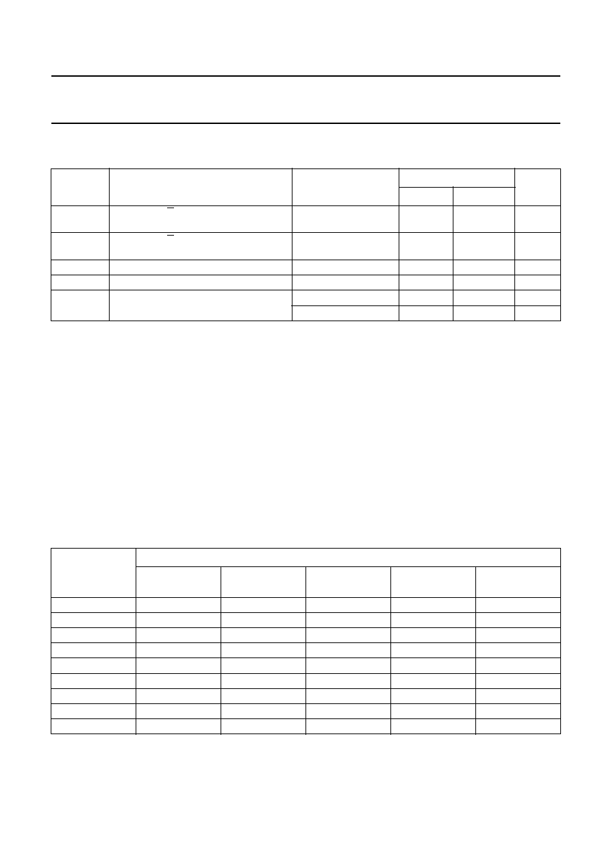
PINNING
PIN
SYMBOL
DESCRIPTION
1
2Y0
independent input or output
2
2Y2
independent input or output
3
2Z
common input or output
4
2Y3
independent input or output
5
2Y1
independent input or output
6
E
enable input (active LOW)
7
V
EE
negative supply voltage
8
GND
ground (0 V)
9
S1
select logic input
10
S0
select logic input
11
1Y3
independent input or output
12
1Y0
independent input or output
13
1Z
common input or output
14
1Y1
independent input or output
15
1Y2
independent input or output
16
V
CC
positive supply voltage
handbook, halfpage
4052
MNB039
1
2
3
4
5
6
7
8
16
15
14
13
12
11
10
9
2Y0
2Y2
2Z
2Y3
2Y1
E
VEE
GND
S1
S0
1Y3
1Y0
1Z
1Y1
1Y2
VCC
Fig.1
Pin configuration DIP16, SO16 and
(T)SSOP16.
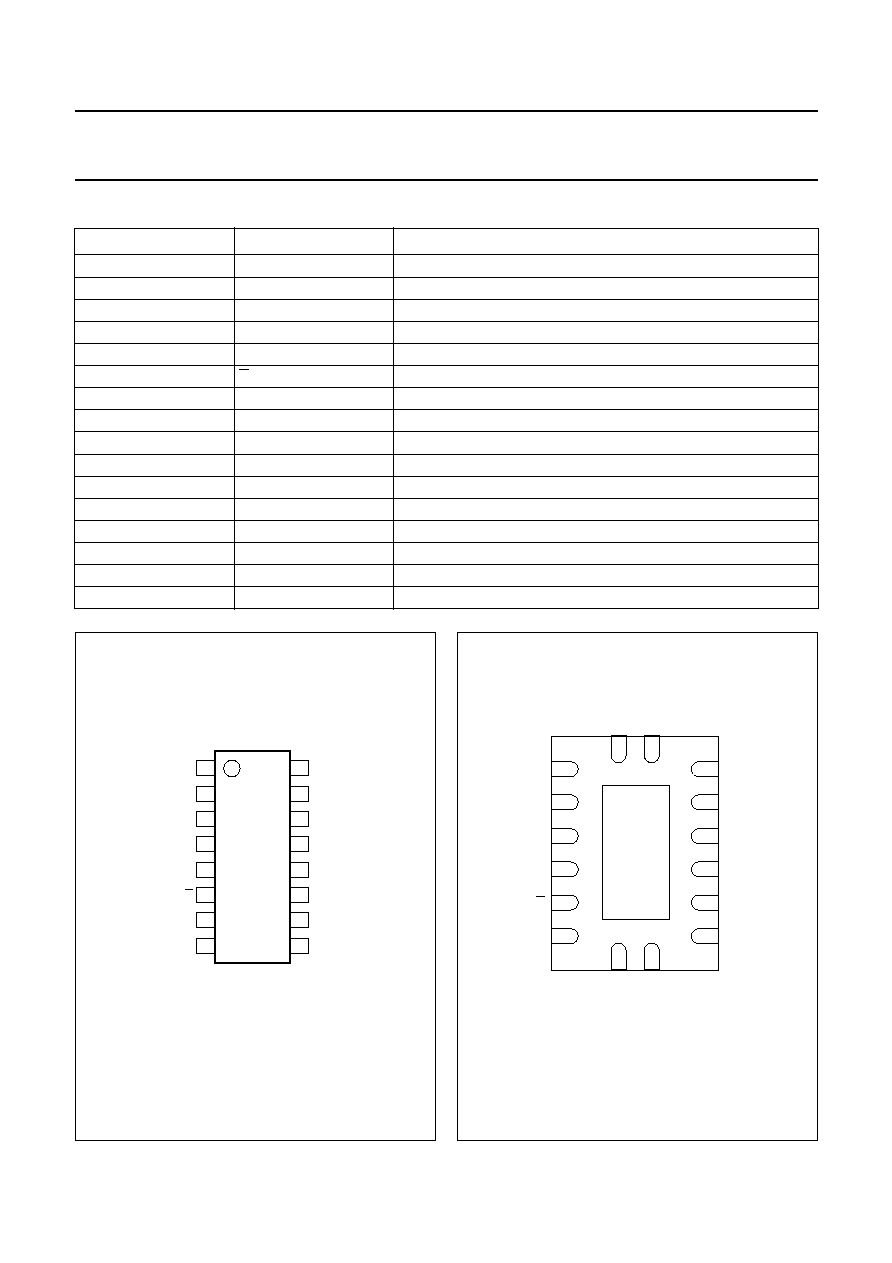
handbook, halfpage
1
16
GND
(1)
2Y0
VCC
8
2
3
4
5
7
2Y2
2Z
2Y3
2Y1
E
15
14
13
12
10
6
11
9
GND
Top view
MNB061
VEE
S1
S0
1Y3
1Y0
1Z
1Y1
1Y2
Fig.2 Pin configuration DHVQFN16.
(1) The die substrate is attached to this pad using conductive die
attach material. It can not be used as a supply pin or input.

2003 May 16
5
Philips Semiconductors
Product specification
Dual 4-channel analog multiplexer,
demultiplexer
74HC4052; 74HCT4052
handbook, halfpage
MNB040
4
2
5
1
11
15
14
12
13
3
6
9
1Z
S0
S1
E
2Z
2Y3
2Y2
2Y1
2Y0
1Y3
1Y2
1Y1
1Y0
10
Fig.3 Logic symbol.
handbook, halfpage
MNB041
11
15
14
12
4
2
5
9
1
10
0
6
G4
MDX
0
3
4
◊
1
3
2
1
0
13
3
Fig.4 IEC logic symbol.
handbook, full pagewidth
MNB042
1 - OF - 4
DECODER
LOGIC
LEVEL
CONVERSION
7
8
VEE
GND
VCC
12
13
16
3
14
15
11
10
9
6
S0
S1
E
1
5
2
1Y0
1Z
2Z
1Y1
1Y2
1Y3
2Y0
2Y1
2Y2
2Y3
4
Fig.5 Functional diagram.