2004 Oct 12
2
Philips Semiconductors
Product specification
4-to-16 line decoder/demultiplexer
74HC154; 74HCT154
FEATURES
∑
16-line demultiplexing capability
∑
Decodes 4 binary-coded inputs into one 16 mutually
exclusive outputs
∑
Complies with JEDEC standard no. 8-1 B
∑
ESD protection:
HBM EIA/JESD22-A114-B exceeds 2000 V
MM EIA/JESD22-A115-A exceeds 200 V.
∑
Specified from
-
40
∞
C to +85
∞
C and
-
40
∞
C to +125
∞
C.
DESCRIPTION
The 74HC154; 74HCT154 are high-speed Si-gate CMOS
devices and are pin compatible with low power Schottky
TTL (LSTTL). They are specified in compliance with
JEDEC standard no. 7A.
The 74HC154; 74HCT154 decoders accept four active
HIGH binary address inputs and provide 16 mutually
exclusive active LOW outputs. The two-input enable gate
can be used to strobe the decoder to eliminate the normal
decoding "glitches" on the outputs, or can be used for the
expansion of the decoder.
The enable gate has two ANDed inputs which must be
LOW to enable the outputs.
The 74HC154; 74HCT154 can be used as a 1-to-16
demultiplexer by using one of the enable inputs as the
multiplexed data input.
When the other enable input is LOW, the addressed output
will follow the state of the applied data.
QUICK REFERENCE DATA
GND = 0 V; T
amb
= 25
∞
C; t
r
= t
f
= 6 ns.
Notes
1. C
PD
is used to determine the dynamic power dissipation (P
D
in
µ
W).
P
D
= C
PD
◊
V
CC
2
◊
f
i
◊
N +
(C
L
◊
V
CC
2
◊
f
o
) where:
f
i
= input frequency in MHz;
f
o
= output frequency in MHz;
C
L
= output load capacitance in pF;
V
CC
= supply voltage in Volts;
N = total load switching outputs;
(C
L
◊
V
CC
2
◊
f
o
) = sum of the outputs.
2. For 74HC154 the condition is V
I
= GND to V
CC
For 74HCT154 the condition is V
I
= GND to V
CC
-
1.5 V.
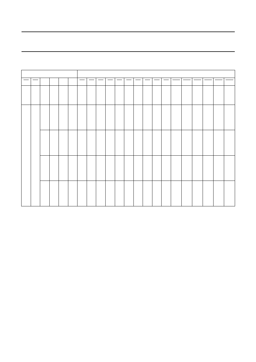
SYMBOL
PARAMETER
CONDITIONS
TYPICAL
UNIT
74HC154
74HCT154
t
PHL
/t
PLH
propagation delay An, En to Yn
C
L
= 15 pF; R
L
= 1 k
;
V
CC
= 5 V
11
13
ns
C
I
input capacitance
3.5
3.5
pF
C
PD
power dissipation capacitance per gate
notes 1 and 2
60
60
pF

2004 Oct 12
5
Philips Semiconductors
Product specification
4-to-16 line decoder/demultiplexer
74HC154; 74HCT154
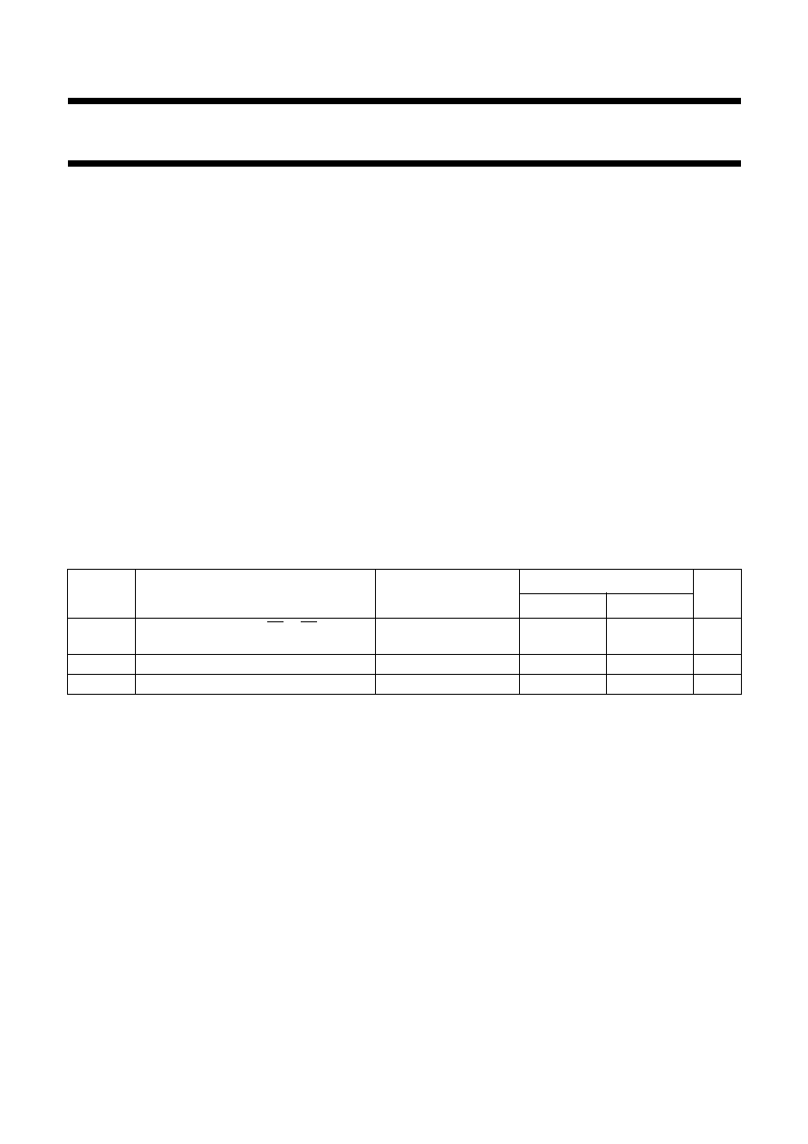
154
Y0
V
CC
Y1
A0
Y2
A1
Y3
A2
Y4
A3
Y5
E1
Y6
E0
Y7
Y15
Y8
Y14
Y9
Y13
Y10
Y12
GND
Y11
001aab067
1
2
3
4
5
6
7
8
9
10
11
12
14
13
16
15
18
17
20
19
22
21
24
23
Fig.1
Pin configuration SO24, DIP24 and
(T)SSOP24.
001aab068
154
Y12
Y9
Y10
Y13
Y8
Y14
Y7
Y15
Y6
E0
Y5
E1
Y4
A3
Y3
A2
Y2
A1
Y1
A0
GND
Y11
Y0
V
CC
11
14
10
15
9
16
8
17
7
18
6
V
CC
(1)
19
5
20
4
21
3
22
2
23
12
13
1
24
terminal 1
index area
Transparent top view
Fig.2 Pin configuration DHVQFN24.
(1) The die substrate is attached to this pad using conductive die
attach material. It can not be used as a supply pin or input.
001aab069
A3
Y15
20
17
Y14
16
Y1
2
Y0
1
A2
21
A1
22
A0
23
18
19
E0
E1
Fig.3 Logic symbol.
001aab070
22
21
3
0
15
DX
20
0
0
G
23
2
3
4
1
2
3
1
5
4
6
5
7
6
8
7
9
8
10
9
11
10
13
11
14
12
15
13
16
14
17
15
18
&
EN
19
22
21
8
X/Y
20
1
2
4
0
23
2
3
4
1
2
3
1
5
4
6
5
7
6
8
7
9
8
10
9
11
10
13
11
14
12
15
13
16
14
17
15
18
&
EN
19
Fig.4 IEC logic symbol.