2003 Jun 17
2
Philips Semiconductors
Product specification
Quad bilateral switches
74HC4066; 74HCT4066
FEATURES
∑
Very low ON-resistance:
≠ 50
(typical) at V
CC
= 4.5 V
≠ 45
(typical) at V
CC
= 6.0 V
≠ 35
(typical) at V
CC
= 9.0 V.
∑
Complies with JEDEC standard no. 8-1A
∑
ESD protection:
HBM EIA/JESD22-A114-A exceeds 2000 V
MM EIA/JESD22-A115-A exceeds 200 V.
∑
Specified from
-
40 to +85
∞
C and
-
40 to +125
∞
C.
GENERAL DESCRIPTION
The 74HC4066 and 74HCT4066 are high-speed Si-gate
CMOS devices and are pin compatible with the
HEF4066B. They are specified in compliance with JEDEC
standard no. 7A.
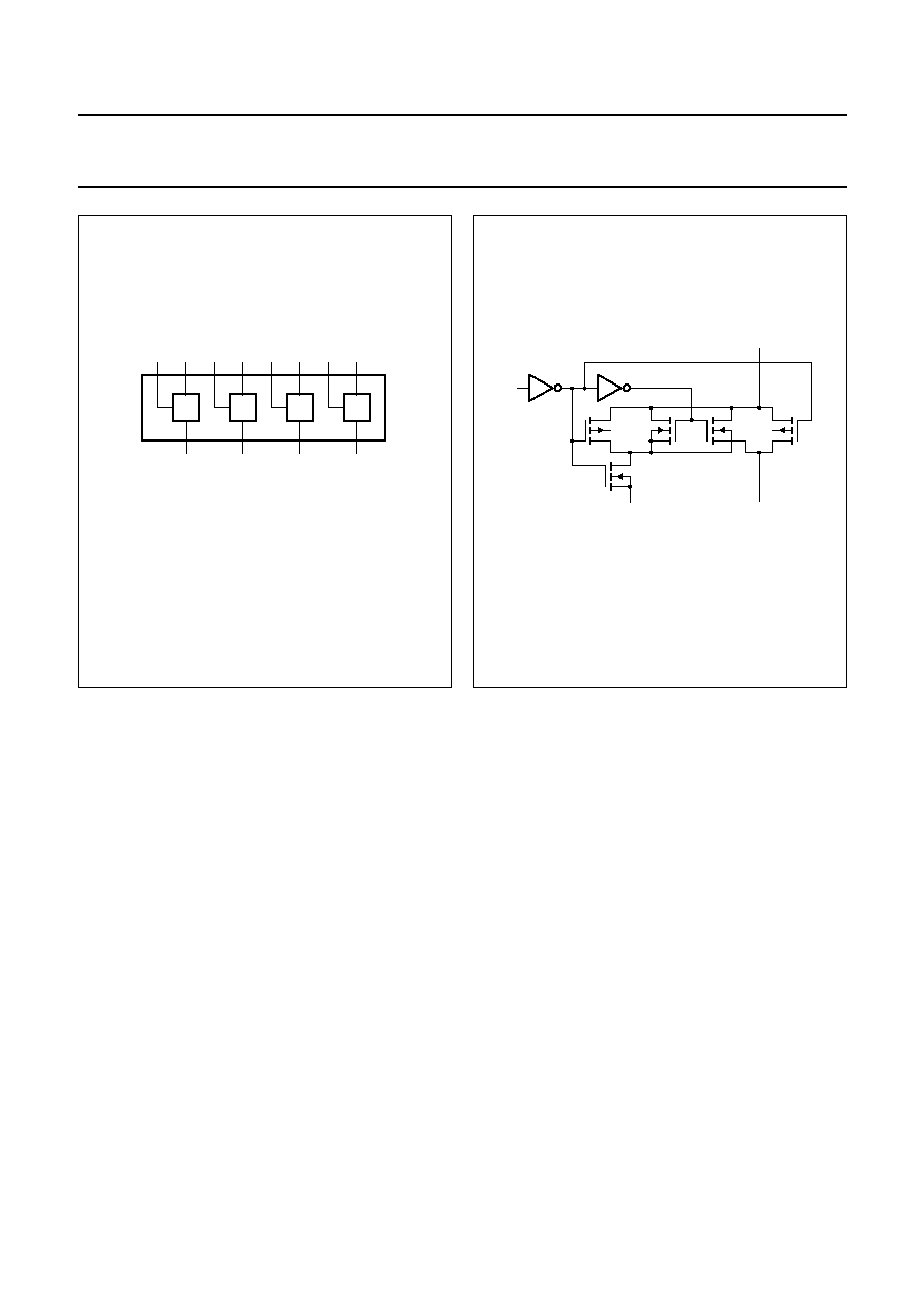
The 74HC4066 and 74HCT4066 have four independent
analog switches. Each switch has two input/output pins
(pins nY or nZ) and an active HIGH enable input pin
(pin nE). When pin nE = LOW the belonging analog switch
is turned off.
The 74HC4066/74HCT4066 is pin compatible with the
74HC4016/74HCT4066 but exhibits a much lower
on-resistance. In addition, the on-resistance is relatively
constant over the full input signal range.
QUICK REFERENCE DATA
GND = 0 V; T
amb
= 25
∞
C; t
r
= t
f
= 6 ns.
Notes
1. C
PD
is used to determine the dynamic power dissipation (P
D
in
µ
W).
P
D
= C
PD
◊
V
CC
2
◊
f
i
◊
N +
[(C
L
+ C
S
)
◊
V
CC
2
◊
f
o
] where:
f
i
= input frequency in MHz;
f
o
= output frequency in MHz;
C
L
= output load capacitance in pF;
C
S
= maximum switch capacitance in pF;
V
CC
= supply voltage in Volts;
N = total load switching outputs;
[(C
L
+ C
S
)
◊
V
CC
2
◊
f
o
] = sum of the outputs.
2. For 74HC4066 the condition is V
I
= GND to V
CC
.
For 74HCT4066 the condition is V
I
= GND to V
CC
-
1.5 V.
SYMBOL
PARAMETER
CONDITIONS
TYPICAL
UNIT
74HC4066
74HCT4066
t
PZH
/t
PZL
turn-on time nE to V
os
C
L
= 15 pF; R
L
= 1 k
; V
CC
= 5 V
11
12
ns
t
PHZ
/t
PLZ
turn-off time nE to V
os
C
L
= 15 pF; R
L
= 1 k
; V
CC
= 5 V
13
16
ns
C
I
input capacitance
3.5
3.5
pF
C
PD
power dissipation
capacitance per switch
notes 1 and 2
11
12
pF
C
S
maximum switch
capacitance
8
8
pF

2003 Jun 17
3
Philips Semiconductors
Product specification
Quad bilateral switches
74HC4066; 74HCT4066
FUNCTION TABLE
See note 1.
Note
1. H = HIGH voltage level.
L = LOW voltage level.
ORDERING INFORMATION
INPUT nE
SWITCH
L
off
H
on
TYPE NUMBER
PACKAGE
TEMPERATURE RANGE
PINS
PACKAGE
MATERIAL
CODE
74HC4066N
-
40 to 125
∞
C
14
DIP14
plastic
SOT27-1
74HCT4066N
-
40 to 125
∞
C
14
DIP14
plastic
SOT27-1
74HC4066D
-
40 to 125
∞
C
14
SO14
plastic
SOT108-1
74HCT4066D
-
40 to 125
∞
C
14
SO14
plastic
SOT108-1
74HC4066DB
-
40 to 125
∞
C
14
SSOP14
plastic
SOT337-1
74HCT4066DB
-
40 to 125
∞
C
14
SSOP14
plastic
SOT337-1
74HC4066PW
-
40 to 125
∞
C
14
TSSOP14
plastic
SOT402-1
74HCT4066PW
-
40 to 125
∞
C
14
TSSOP14
plastic
SOT402-1
74HC4066BQ
-
40 to 125
∞
C
14
DHVQFN14
plastic
SOT762-1
74HCT4066BQ
-
40 to 125
∞
C
14
DHVQFN14
plastic
SOT762-1
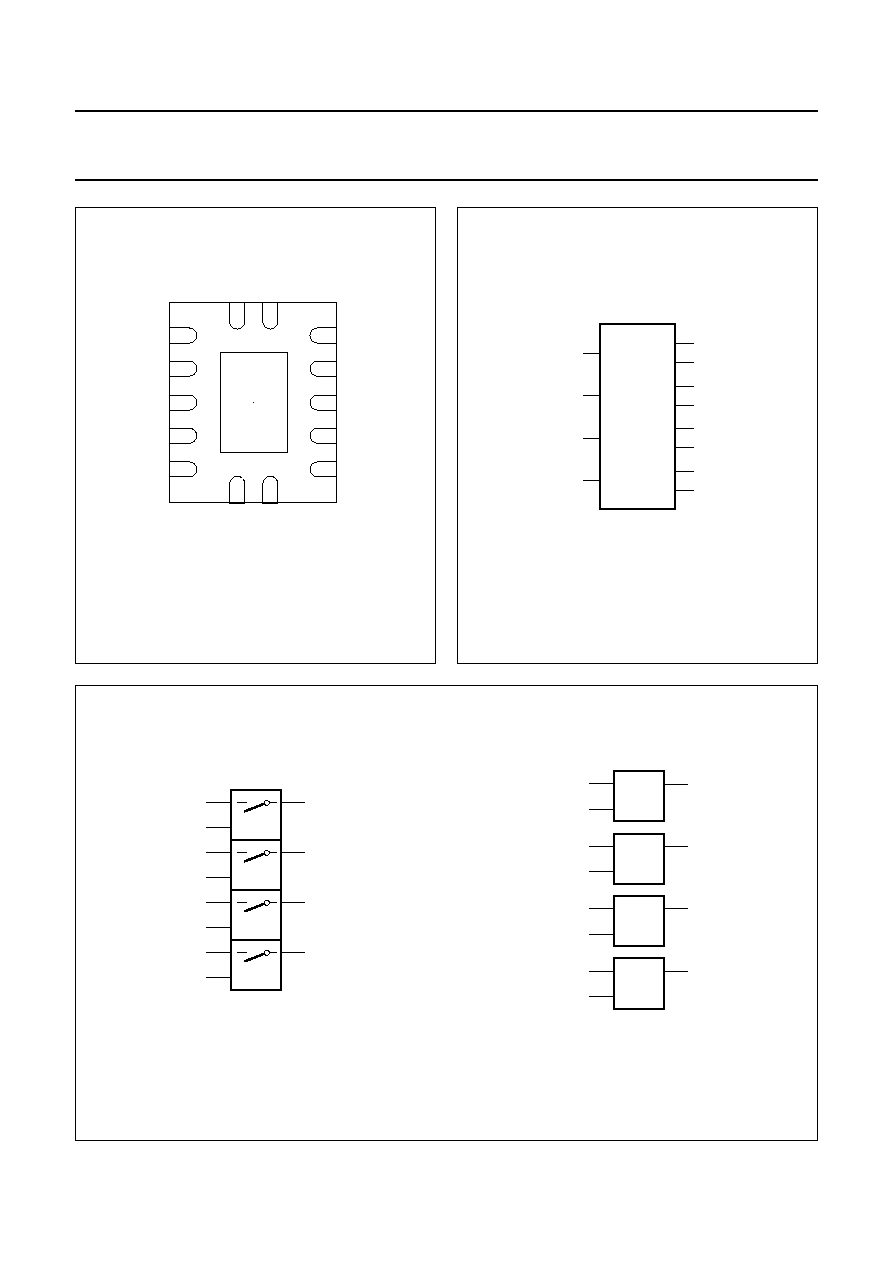
PINNING
PIN
SYMBOL
DESCRIPTION
1
1Y
independent input/output
2
1Z
independent input/output
3
2Z
independent input/output
4
2Y
independent input/output
5
2E
enable input (active HIGH)
6
3E
enable input (active HIGH)
7
GND
ground (0 V)
8
3Y
independent input/output
9
3Z
independent input/output
10
4Z
independent input/output
11
4Y
independent input/output
12
4E
enable input (active HIGH)
13
1E
enable input (active HIGH)
14
V
CC
supply voltage
handbook, halfpage
MGR253
4066
1
2
3
4
5
6
7
8
14
13
12
11
10
9
1Y
1Z
2Z
2Y
2E
3E
GND
3Y
3Z
4Z
4Y
4E
1E
VCC
Fig.1
Pin configuration DIP14, SO14 and
(T)SSOP14.
2003 Jun 17
4
Philips Semiconductors
Product specification
Quad bilateral switches
74HC4066; 74HCT4066
handbook, halfpage
1
14
1Y
VCC
7
2
3
4
5
6
1Z
2Z
2Y
2E
3E
13
12
11
10
9
1E
4E
4Y
4Z
3Z
8
GND
3Y
MBL891
GND
(1)
Top view
Fig.2 Pin configuration DHVQFN14.
(1) The die substrate is attached to this pad using conductive die
attach material. It can not be used as a supply pin or input.
handbook, halfpage
MGR254
13
1
1Y
2
1Z
4
2Y
3
2Z
8
3Y
9
3Z
11
4Y
10
4Z
1E
5
2E
6
3E
12
4E
Fig.3 Logic symbol.
handbook, halfpage
MGR255
13 #
5 #
6 #
12 #
1
2
4
3
8
9
11
10
handbook, halfpage
MGR256
13 #
5 #
6 #
12 #
1
1
1
X1
1
1
X1
1
1
X1
1
1
X1
2
4
3
8
9
11
10
Fig.4 IEC logic symbol.