 | ÐлекÑÑоннÑй компоненÑ: 74HC4067 | СкаÑаÑÑ:  PDF PDF  ZIP ZIP |
Äîêóìåíòàöèÿ è îïèñàíèÿ www.docs.chipfind.ru

DATA SHEET
Product specification
File under Integrated Circuits, IC06
September 1993
INTEGRATED CIRCUITS
74HC/HCT4067
16-channel analog
multiplexer/demultiplexer
For a complete data sheet, please also download:
·
The IC06 74HC/HCT/HCU/HCMOS Logic Family Specifications
·
The IC06 74HC/HCT/HCU/HCMOS Logic Package Information
·
The IC06 74HC/HCT/HCU/HCMOS Logic Package Outlines
September 1993
2
Philips Semiconductors
Product specification
16-channel analog
multiplexer/demultiplexer
74HC/HCT4067
FEATURES
·
Low "ON" resistance:
80
(typ.) at V
CC
= 4.5 V
70
(typ.) at V
CC
= 6.0 V
60
(typ.) at V
CC
= 9.0 V
typical "break before make" built-in
·
Output capability: non-standard
·
I
CC
category: MSI
GENERAL DESCRIPTION
The 74HC/HCT4067 are high-speed Si-gate CMOS
devices and are pin compatible with the "4067" of the
"4000B" series. They are specified in compliance with
JEDEC standard no. 7A.
The 74HC/HCT4067 are 16-channel analog
multiplexers/demultiplexers with four address inputs (S
0
to
S
3
) , an active LOW enable input (E), sixteen independent
inputs/outputs (Y
0
to Y
15
) and a common input/output (Z).
The "4067" contains sixteen bidirectional analog switches,
each with one side connected to an independent
input/output (Y
0
to Y
15
) and the other side connected to a
common input/output (Z).
With E LOW, one of the sixteen switches is selected (low
impedance ON-state) by S
0
to S
3
. All unselected switches
are in the high impedance OFF-state. With E HIGH, all
switches are in the high impedance OFF-state,
independent of S
0
to S
3
.
The analog inputs/outputs (Y
0
to Y
15
, and Z) can swing
between V
CC
as a positive limit and GND as a negative
limit. V
CC
to GND may not exceed 10 V.
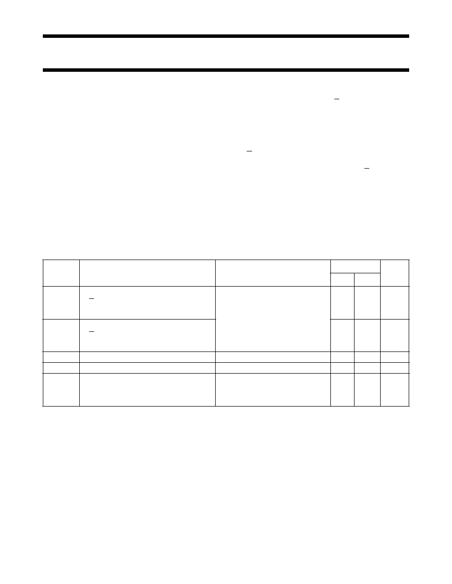
QUICK REFERENCE DATA
GND = 0 V; T
amb
= 25
°
C; t
r
= t
f
= 6 ns
Notes
1. C
PD
is used to determine the dynamic power dissipation (P
D
in
µ
W):
P
D
= C
PD
×
V
CC
2
×
f
i
+ {
(C
L
+
C
S
)
×
V
CC
2
×
f
o
} where:
f
i
= input frequency in MHz
f
o
= output frequency in MHz
{(C
L
+
C
S
)
×
V
CC
2
×
f
o
} = sum of outputs
C
L
= output load capacitance in pF
C
S
= max. switch capacitance in pF
V
CC
= supply voltage in V
2. For HC the condition is V
I
= GND to V
CC
For HCT the condition is V
I
= GND to V
CC
-
1.5 V
SYMBOL
PARAMETER
CONDITIONS
TYPICAL
UNIT
HC
HCT
t
PZL
/ t
PZH
turn-on time
C
L
= 15 pF; R
L
= 1 k
; V
CC
= 5 V
E to V
os
26
32
ns
S
n
to V
os
29
33
ns
t
PLZ
/ t
PHZ
turn-off time
E to V
os
27
26
ns
S
n
to V
os
29
30
ns
C
I
input capacitance
3.5
3.5
pF
C
PD
power dissipation capacitance per switch
notes 1 and 2
29
29
pF
C
S
max. switch capacitance
independent (Y)
5
5
pF
common (Z)
45
45
pF
September 1993
3
Philips Semiconductors
Product specification
16-channel analog
multiplexer/demultiplexer
74HC/HCT4067
ORDERING INFORMATION
See
"74HC/HCT/HCU/HCMOS Logic Package Information"
.
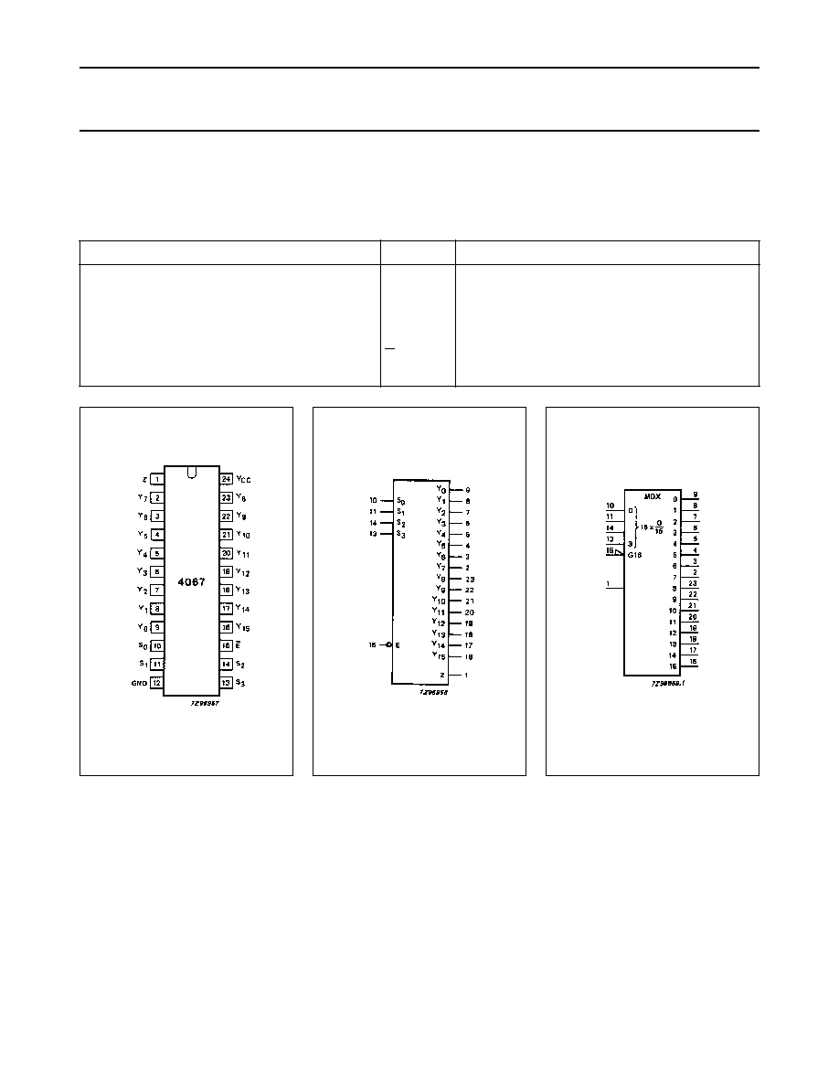
PIN DESCRIPTION
PIN NO.
SYMBOL
NAME AND FUNCTION
1
Z
common input/output
9, 8, 7, 6, 5, 4, 3, 2, 23, 22, 21, 20, 19, 18, 17, 16
Y
0
to Y
15
independent inputs/outputs
10, 11, 14, 13
S
0
to S
3
address inputs
12
GND
ground (0 V)
15
E
enable input (active LOW)
24
V
CC
positive supply voltage
Fig.1 Pin configuration.
Fig.2 Logic symbol.
Fig.3 IEC logic symbol.
September 1993
4
Philips Semiconductors
Product specification
16-channel analog
multiplexer/demultiplexer
74HC/HCT4067
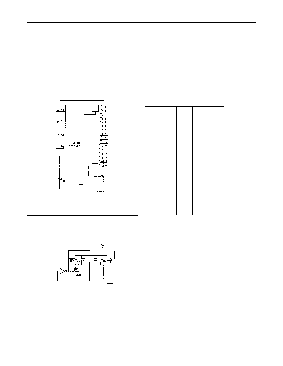
APPLICATIONS
·
Analog multiplexing and demultiplexing
·
Digital multiplexing and demultiplexing
·
Signal gating
Fig.4 Functional diagram.
Fig.5 Schematic diagram (one switch).
FUNCTION TABLE
Notes
1. H = HIGH voltage level
L = LOW voltage level
X = don't care
INPUTS
CHANNEL
ON
E
S
3
S
2
S
1
S
0
L
L
L
L
L
L
L
L
L
L
L
L
L
L
H
H
L
H
L
H
Y
0
-
Z
Y
1
-
Z
Y
2
-
Z
Y
3
-
Z
L
L
L
L
L
L
L
L
H
H
H
H
L
L
H
H
L
H
L
H
Y
4
-
Z
Y
5
-
Z
Y
6
-
Z
Y
7
-
Z
L
L
L
L
H
H
H
H
L
L
L
L
L
L
H
H
L
H
L
H
Y
8
-
Z
Y
9
-
Z
Y
10
-
Z
Y
11
-
Z
L
L
L
L
H
H
H
H
H
H
H
H
L
L
H
H
L
H
L
H
Y
12
-
Z
Y
13
-
Z
Y
14
-
Z
Y
15
-
Z
H
X
X
X
X
none
September 1993
5
Philips Semiconductors
Product specification
16-channel analog
multiplexer/demultiplexer
74HC/HCT4067
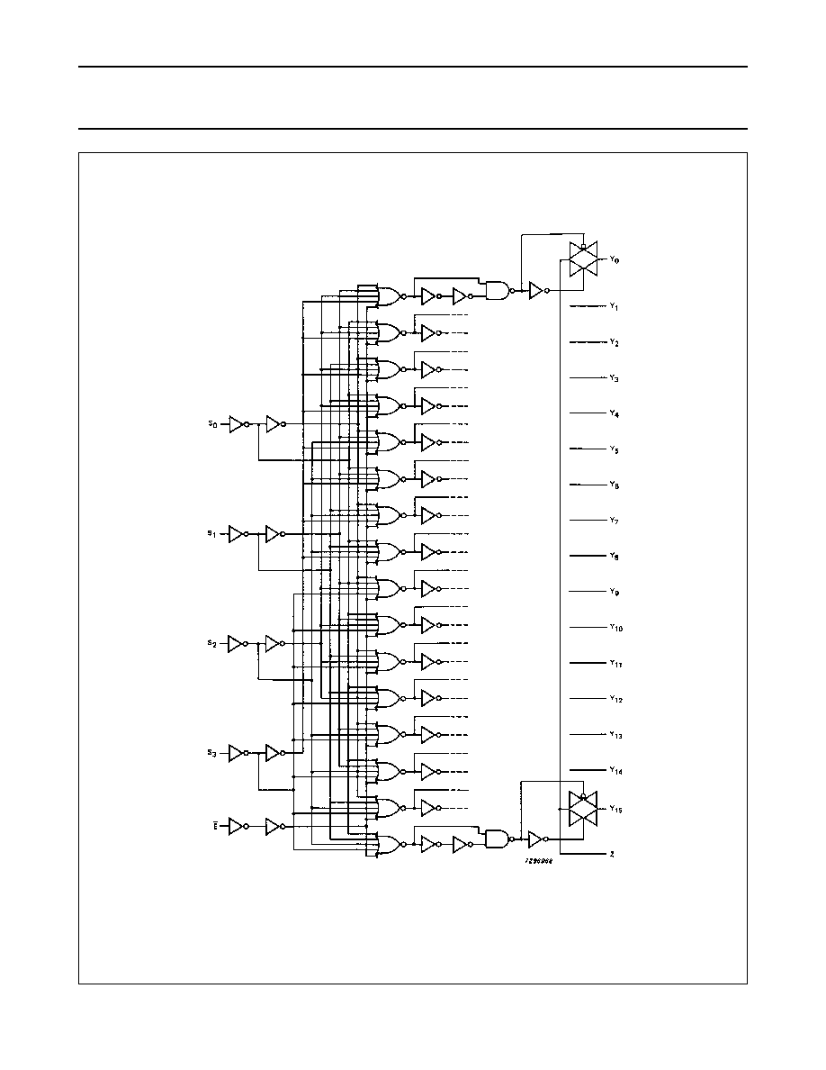
Fig.6 Logic diagram.
September 1993
6
Philips Semiconductors
Product specification
16-channel analog
multiplexer/demultiplexer
74HC/HCT4067
RATINGS
Limiting values in accordance with the Absolute Maximum System (IEC 134)
Voltages are referenced to GND (ground = 0 V)
Note
1. To avoid drawing V
CC
current out of terminal Z, when switch current flows in terminals Y
n
, the voltage drop across
the bidirectional switch must not exceed 0.4 V. If the switch current flows into terminal Z, no V
CC
current will flow out
of terminals Y
n
. In this case there is no limit for the voltage drop across the switch, but the voltages at Y
n
and Z may
not exceed V
CC
or GND.
RECOMMENDED OPERATING CONDITIONS
SYMBOL
PARAMETER
MIN.
MAX.
UNIT
CONDITIONS
V
CC
DC supply voltage
-
0.5
+
11.0
V
±
I
IK
DC digital input diode current
20
mA
for V
I
< -
0.5 or V
I
>
V
CC
+
0.5 V
±
I
SK
DC switch diode current
20
mA
for V
S
< -
0.5 or V
S
>
V
CC
+
0.5 V
±
I
S
DC switch current
25
mA
for
-
0.5 V
<
V
S
<
V
CC
+
0.5 V
±
I
CC
;
±
I
GND
DC V
CC
or GND current
50
mA
T
stg
storage temperature range
-
65
+
150
°
C
P
tot
power dissipation per package
for temperature range:
-
40 to
+
125
°
C
74HC/HCT
plastic DIL
750
mW
above
+
70
°
C: derate linearly with 12 mW/K
plastic mini-pack (SO)
500
mW
above
+
70
°
C: derate linearly with 8 mW/K
P
S
power dissipation per switch
100
mW
SYMBOL PARAMETER
74HC
74HCT
UNIT
CONDITIONS
min.
typ. max. min.
typ. max.
V
CC
DC supply voltage
2.0
5.0
10.0
4.5
5.0
5.5
V
V
I
DC input voltage range
GND
V
CC
GND
V
CC
V
V
S
DC switch voltage range
GND
V
CC
GND
V
CC
V
T
amb
operating ambient temperature range
-
40
+
85
-
40
+
85
°
C
see DC and AC
CHARACTER-
ISTICS
T
amb
operating ambient temperature range
-
40
+
125
-
40
+
125
°
C
t
r
, t
f
input rise and fall times
6.0
1000
500
400
250
6.0
500
ns
V
CC
= 2.0 V
V
CC
= 4.5 V
V
CC
= 6.0 V
V
CC
= 10.0 V
September 1993
7
Philips Semiconductors
Product specification
16-channel analog
multiplexer/demultiplexer
74HC/HCT4067
DC CHARACTERISTICS FOR 74HC/HCT
For 74HC:
V
CC
-
GND = 2.0, 4.5, 6.0 and 9.0 V
For 74HCT: V
CC
-
GND = 4.5 V
Notes
1. At supply voltages (V
CC
-
GND) approaching 2 V, the analog switch ON-resistance becomes extremely non-linear.
Therefore it is recommended that these devices be used to transmit digital signals only, when using these supply
voltages.
2. For test circuit measuring R
ON
see Fig.7.
SYMBOL
PARAMETER
T
amb
(
°
C)
UNIT
TEST CONDITIONS
74HC/HCT
V
CC
(V)
I
S
(
µ
A)
V
is
V
I
+
25
-
40 to
+
85
-
40 to
+
125
min.
typ.
max.
min.
max.
min.
max.
R
ON
ON-resistance
(peak)
-
110
95
75
-
180
160
130
-
225
200
165
-
270
240
195
2.0
4.5
6.0
9.0
100
1000
1000
1000
V
CC
to
GND
V
IH
or
V
IL
R
ON
ON-resistance (rail)
150
90
80
70
-
160
140
120
-
200
175
150
-
240
210
180
2.0
4.5
6.0
9.0
100
1000
1000
1000
GND
or
V
CC
V
IH
or
V
IL
R
ON
maximum variation
of ON-resistance
between any two
channels
-
9
8
6
2.0
4.5
6.0
9.0
V
CC
to
GND
V
IH
or
V
IL
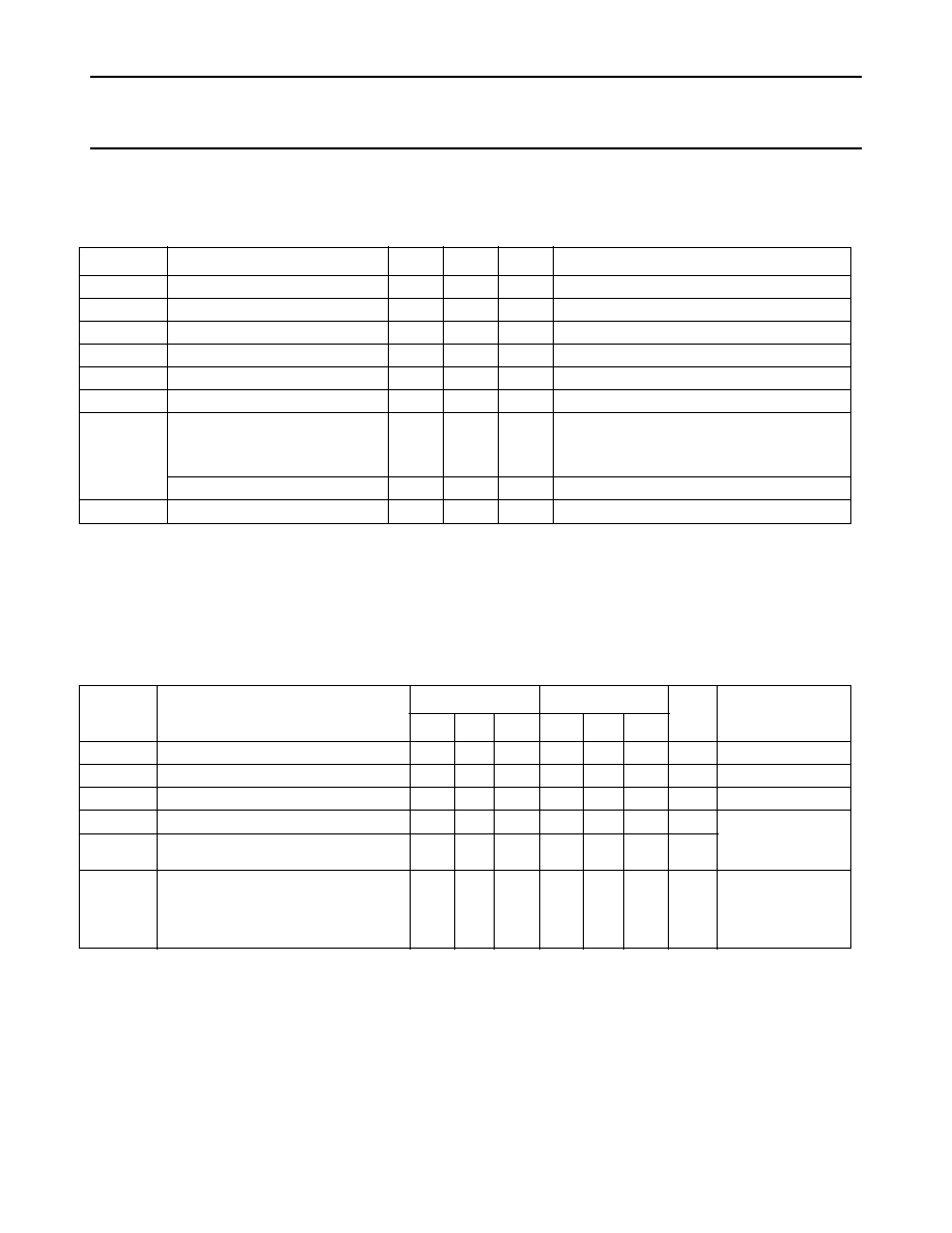
Fig.7 Test circuit for measuring ON-resistance (R
ON
).
Fig.8 Test circuit for measuring OFF-state current.
September 1993
8
Philips Semiconductors
Product specification
16-channel analog
multiplexer/demultiplexer
74HC/HCT4067
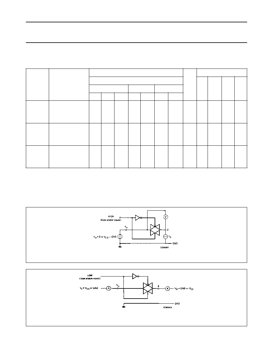
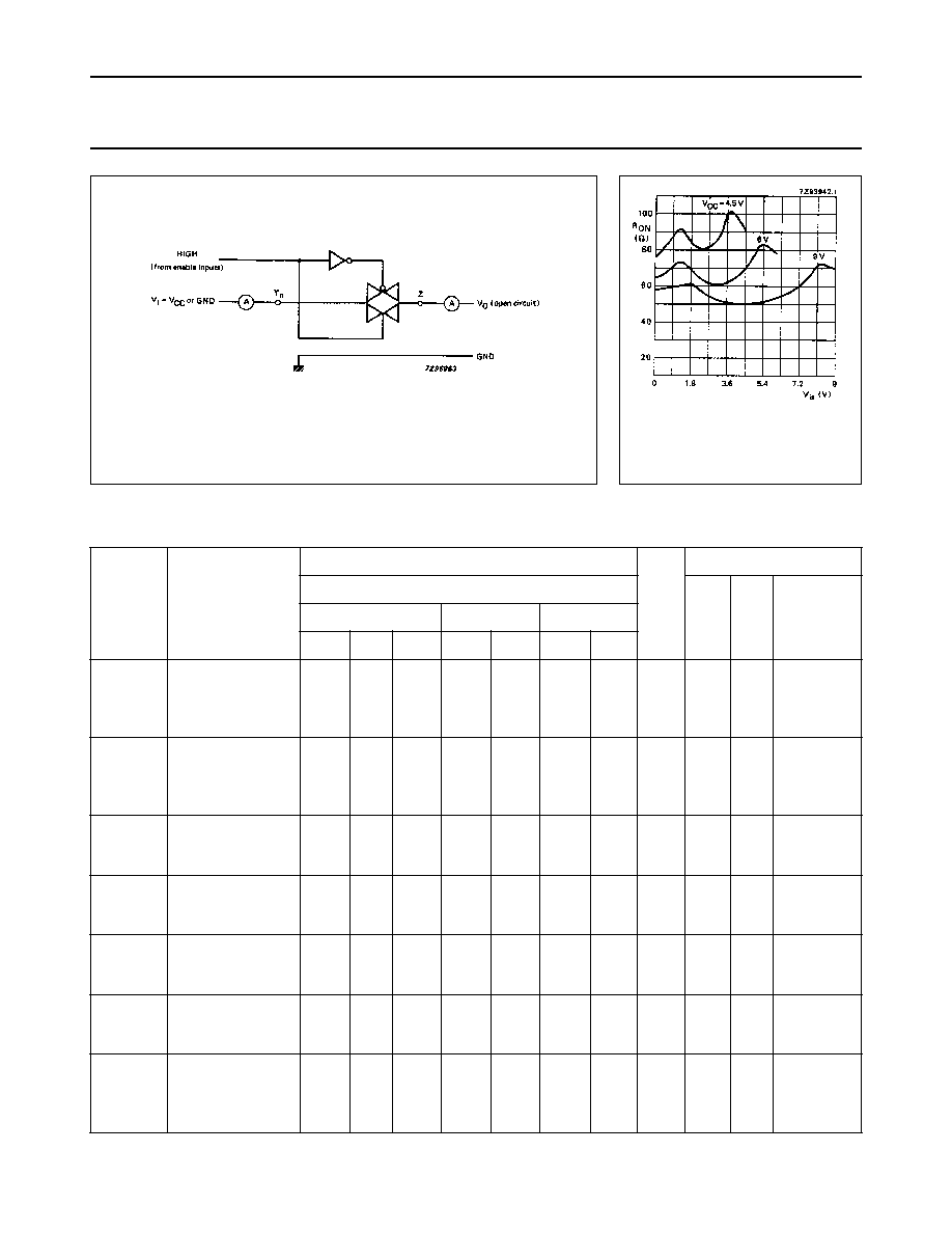
Fig.9 Test circuit for measuring ON-state current.
Fig.10 Typical ON-resistance
(R
ON
) as a function of
input voltage (V
is
) for
V
is
= 0 to V
CC
-
GND.
DC CHARACTERISTICS FOR 74HC
Voltages are referenced to GND (ground = 0 V)
SYMBOL
PARAMETER
T
amb
(
°
C)
UNIT
TEST CONDITIONS
74HC
V
CC
(V)
V
I
OTHER
+
25
-
40 to
+
85
-
40 to
+
125
min.
typ.
max.
min.
max.
min.
max.
V
IH
HIGH level input
voltage
1.5
3.15
4.2
6.3
1.2
2.4
3.2
4.7
1.5
3.15
4.2
6.3
1.5
3.15
4.2
6.3
V
2.0
4.5
6.0
9.0
V
IL
LOW level input
voltage
0.8
2.1
2.8
4.3
0.50
1.35
1.80
2.70
0.50
1.35
1.80
2.70
0.50
1.35
1.80
2.70
V
2.0
4.5
6.0
9.0
±
I
I
input leakage
current
0.1
0.2
1.0
2.0
1.0
2.0
µ
A
6.0
10.0
V
CC
or
GND
±
I
S
analog switch
OFF-state current
per channel
0.1
1.0
1.0
µ
A
10.0
V
IH
or
V
IL
V
S
=
V
CC
-
GND
(see Fig.8)
±
I
S
analog switch
OFF-state current
all channels
0.8
8.0
8.0
µ
A
10.0
V
IH
or
V
IL
V
S
=
V
CC
-
GND
(see Fig.9)
±
I
S
analog switch
ON-state current
0.8
8.0
8.0
µ
A
10.0
V
IH
or
V
IL
V
S
=
V
CC
-
GND
(see Fig.9)
I
CC
quiescent supply
current
8.0
16.0
80.0
160
160
320
µ
A
6.0
10.0
V
CC
or
GND
V
is
= GND
or V
CC
;
V
os
= V
CC
or GND
September 1993
9
Philips Semiconductors
Product specification
16-channel analog
multiplexer/demultiplexer
74HC/HCT4067
AC CHARACTERISTICS FOR 74HC
GND = 0 V; t
r
= t
f
= 6 ns; C
L
= 50 pF
SYMBOL PARAMETER
T
amb
(
°
C)
UNIT
TEST CONDITIONS
74HC
V
CC
(V)
OTHER
+
25
-
40 to
+
85
-
40 to
+
125
min.
typ. max. min.
max.
min.
max.
t
PHL
/ t
PLH
propagation delay
V
is
to V
os
;
Y
n
to Z
25
9
7
5
75
15
13
9
95
19
16
11
110
22
19
14
ns
2.0
4.5
6.0
9.0
R
L
=
;
C
L
= 50 pF
(see Fig.16)
t
PHL
/ t
PLH
propagation delay
V
is
to V
os
;
Z to Y
n
18
6
5
4
60
12
10
8
75
15
13
10
90
18
15
12
ns
2.0
4.5
6.0
9.0
t
PHZ
/ t
PLZ
turn-off time
E to Y
n
74
27
22
20
250
50
43
38
315
63
54
48
375
75
64
57
ns
2.0
4.5
6.0
9.0
R
L
= 1 k
;
C
L
= 50 pF
(see Fig.17)
t
PHZ
/ t
PLZ
turn-off time
S
n
to Y
n
83
30
24
21
250
50
43
38
315
63
54
48
375
75
64
57
ns
2.0
4.5
6.0
9.0
t
PHZ
/ t
PLZ
turn-off time
E to Z
85
31
25
24
275
55
47
42
345
69
59
53
415
83
71
63
ns
2.0
4.5
6.0
9.0
t
PHZ
/ t
PLZ
turn-off time
S
n
to Z
94
34
27
25
290
58
47
45
365
73
62
56
435
87
74
68
ns
2.0
4.5
6.0
9.0
t
PZH
/ t
PZL
turn-on time
E to Y
n
80
29
23
17
275
55
47
42
345
69
59
53
415
83
71
63
ns
2.0
4.5
6.0
9.0
t
PZH
/ t
PZL
turn-on time
S
n
to Y
n
88
32
26
18
300
60
51
45
375
75
64
56
450
90
77
68
ns
2.0
4.5
6.0
9.0
t
PZH
/ t
PZL
turn-on time
E to Z
85
31
25
18
275
55
47
42
345
69
59
53
415
83
71
63
ns
2.0
4.5
6.0
9.0
t
PZH
/ t
PZL
turn-on time
S
n
to Z
94
34
27
19
300
60
51
45
375
75
64
56
450
90
77
68
ns
2.0
4.5
6.0
9.0
September 1993
10
Philips Semiconductors
Product specification
16-channel analog
multiplexer/demultiplexer
74HC/HCT4067
Note to AC CHARACTERISTICS FOR 74HC
1. Due to higher Z terminal capacitance (16 switches versus 1) the delay figures to the Z terminal are higher than those
to the Y terminal.
DC CHARACTERISTICS FOR 74HCT
Voltages are referenced to GND (ground = 0 V)
Note
1. The value of additional quiescent supply current (
I
CC
) for a unit load of 1 is given here.
To determine
I
CC
per input, multiply this value by the unit load coefficient shown in the table below.
SYMBOL
PARAMETER
T
amb
(
°
C)
UNIT
TEST CONDITIONS
74HCY
V
CC
(V)
V
I
OTHER
+
25
-
40 to
+
85
-
40 to
+
125
min. typ. max. min.
max.
min. max.
V
IH
HIGH level input
voltage
2.0
1.6
2.0
2.0
V
4.5
to
5.5
V
IL
LOW level input
voltage
1.2
0.8
0.8
0.8
V
4.5
to
5.5
±
I
I
input leakage current
0.1
1.0
1.0
µ
A
5.5
V
CC
or
GND
±
I
S
analog switch
OFF-state current per
channel
0.1
1.0
1.0
µ
A
5.5
V
IH
or
V
IL
V
S
=
V
CC
-
GND
(see Fig.8)
±
I
S
analog switch
OFF-state current
all channels
0.8
8.0
8.0
µ
A
5.5
V
IH
or
V
IL
V
S
=
V
CC
-
GND
(see Fig.9)
±
I
S
analog switch
ON-state current
0.8
8.0
8.0
µ
A
5.5
V
IH
or
V
IL
V
S
=
V
CC
-
GND
(see Fig.9)
I
CC
quiescent supply
current
8.0
80.0
160
µ
A
4.5
to
5.5
V
CC
or
GND
V
is
= GND or
V
CC
; V
os
= V
CC
or GND
I
CC
additional quiescent
supply current per
input pin for unit load
coefficient is 1
(note 1)
100 360
450
490
µ
A
4.5
to
5.5
V
CC
-
2.1
V
other inputs at
V
CC
or GND
INPUT
UNIT LOAD COEFFICIENT
E
S
n
0.6
0.5
September 1993
11
Philips Semiconductors
Product specification
16-channel analog
multiplexer/demultiplexer
74HC/HCT4067
AC CHARACTERISTICS FOR 74HCT
GND = 0 V; t
r
= t
f
= 6 ns
Note
1. Due to higher Z terminal capacitance (16 switches versus 1) the delay figures to the Z terminal are higher than those
to the Y terminal.
SYMBOL PARAMETER
T
amb
(
°
C)
UNIT
TEST CONDITIONS
74HCT
V
CC
(V)
OTHER
+
25
-
40 to
+
85
-
40 to
+
125
min.
typ. max. min.
max.
min.
max.
t
PHL
/ t
PLH
propagation delay
V
is
to V
os
;
Y
n
to Z
9
15
19
22
ns
4.5
R
L
=
;
C
L
= 50 pF
(see Fig.16)
t
PHL
/ t
PLH
propagation delay
V
is
to V
os
;
Z to Y
n
6
12
15
18
ns
4.5
t
PHZ
/ t
PLZ
turn-off time
E to Y
n
26
55
69
83
ns
4.5
R
L
= 1 k
;
C
L
= 50 pF
(see Fig.17)
t
PHZ
/ t
PLZ
turn-off time
S
n
to Y
n
31
55
69
83
ns
4.5
t
PHZ
/ t
PLZ
turn-off time
E to Z
30
60
75
90
ns
4.5
t
PHZ
/ t
PLZ
turn-off time
S
n
to Z
35
60
75
90
ns
4.5
t
PZH
/ t
PZL
turn-on time
E to Y
n
32
60
75
90
ns
4.5
t
PZH
/ t
PZL
turn-on time
S
n
to Y
n
35
60
75
90
ns
4.5
t
PZH
/ t
PZL
turn-on time
E to Z
38
65
81
98
ns
4.5
t
PZH
/ t
PZL
turn-on time
S
n
to Z
38
65
81
98
ns
4.5
September 1993
12
Philips Semiconductors
Product specification
16-channel analog
multiplexer/demultiplexer
74HC/HCT4067
ADDITIONAL AC CHARACTERISTICS FOR 74HC/HCT
Recommended conditions and typical values
GND = 0 V; t
r
= t
f
= 6 ns
Notes
1. V
is
is the input voltage at Y
n
or Z terminal, whichever is assigned as an input.
2. V
os
is the output voltage at Y
n
or Z terminal, whichever is assigned as an output.
3. Adjust input voltage V
is
is 0 dBm level (0 dBm = 1 mW into 600
).
4. Adjust input voltage V
is
is 0 dBm level at V
os
for 1 MHz (0 dBm = 1 mW into 50
).
SYMBOL
PARAMETER
TYP.
UNIT
V
CC
(V)
V
is(p-p)
(V)
CONDITIONS
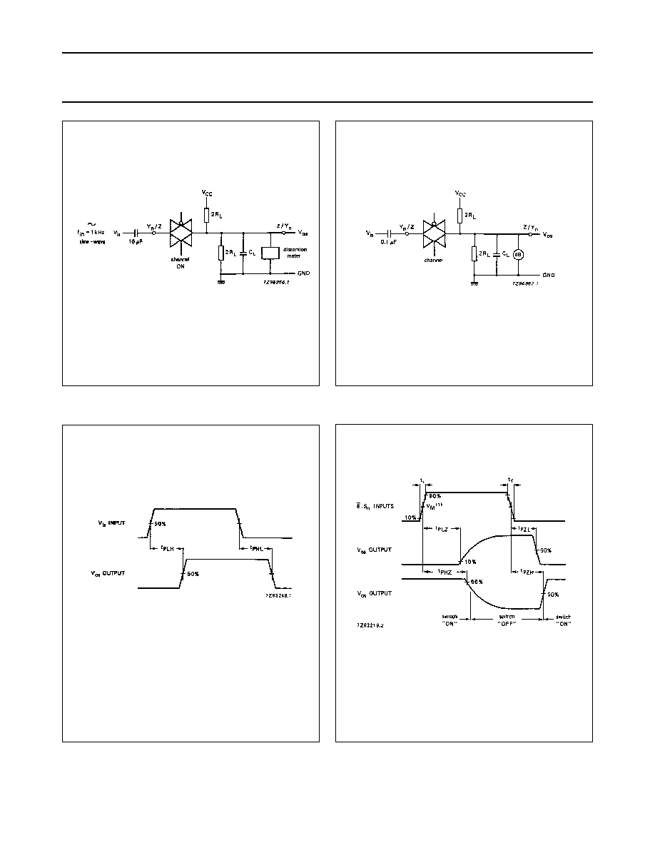
sine-wave distortion
f = 1 kHz
0.04
0.02
%
%
4.5
9.0
4.0
8.0
R
L
= 10 k
; C
L
= 50 pF
(see Fig.14)
sine-wave distortion
f = 10 kHz
0.12
0.06
%
%
4.5
9.0
4.0
8.0
R
L
= 10 k
; C
L
= 50 pF
(see Fig.14)
switch "OFF" signal
feed-through
-
50
-
50
dB
dB
4.5
9.0
note 3
R
L
= 600
; C
L
= 50 pF
f = 1 MHz (see Figs 11 and 15)
f
max
minimum frequency response
(
-
3 dB)
90
100
MHz
MHz
4.5
9.0
note 4
R
L
= 50
; C
L
= 10 pF
(see Figs 12 and 13)
C
S
maximum switch capacitance
independent (Y)
common (Z)
5
45
pF
pF
September 1993
13
Philips Semiconductors
Product specification
16-channel analog
multiplexer/demultiplexer
74HC/HCT4067
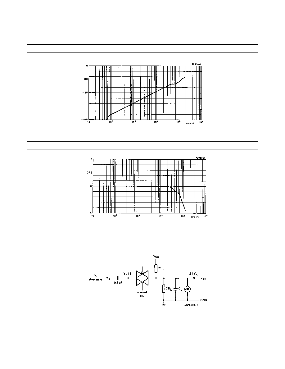
Fig.11 Typical switch "OFF" signal feed-through as a function of frequency.
Test conditions:
V
CC
= 4.5 V; GND = 0 V;
R
L
= 50
; R
source
= 1 k
.
Fig.12 Typical frequency response.
Test conditions:
V
CC
= 4.5 V; GND = 0 V;
R
L
= 50
; R
source
= 1 k
.
Fig.13 Test circuit for measuring minimum frequency response.
Adjust input voltage to obtain
0 dBm at V
os
when f
in
= 1 MHz.
After set-up frequency of f
in
is
increased to obtain a reading of
-
3 dB at V
os
.
September 1993
14
Philips Semiconductors
Product specification
16-channel analog
multiplexer/demultiplexer
74HC/HCT4067
Fig.14 Test circuit for measuring sine-wave
distortion.
Fig.15 Test circuit for measuring switch "OFF"
signal feed-through.
AC WAVEFORMS
Fig.16 Waveforms showing the input (V
is
) to output
(V
os
) propagation delays.
Fig.17 Waveforms showing the turn-on and
turn-off times.
(1) HC : V
M
= 50%; V
I
= GND to V
CC
.
HCT : V
M
= 1.3 V; V
I
= GND to 3 V.
September 1993
15
Philips Semiconductors
Product specification
16-channel analog
multiplexer/demultiplexer
74HC/HCT4067
TEST CIRCUIT AND WAVEFORMS
PACKAGE OUTLINES
See
"74HC/HCT/HCU/HCMOS Logic Package Outlines"
.
Fig.18 Test circuit for measuring AC performance.
Conditions
TEST
SWITCH
V
is
t
PZH
t
PZL
t
PHZ
t
PLZ
others
GND
V
CC
GND
V
CC
open
V
CC
GND
V
CC
GND
pulse
C
L
=
load capacitance including jig and
probe capacitance (see AC
CHARACTERISTICS for values).
R
T
=
termination resistance should be equal
to the output impedance Z
O
of the
pulse generator.
t
r
=
t
f
= 6 ns, when measuring f
max
, there is
no constraint on t
r
, t
f
with 50% duty
factor.
Fig.19 Input pulse definitions.
FAMILY
AMPLI-
TUDE
V
M
t
r
, t
f
f
max
;
PULSE WIDTH
OTHER
74HC
V
CC
50%
<
2 ns
6 ns
74HCT
3.0 V
1.3 V
<
2 ns
6 ns