 | –≠–ª–µ–∫—Ç—Ä–æ–Ω–Ω—ã–π –∫–æ–º–ø–æ–Ω–µ–Ω—Ç: 74HC42DB | –°–∫–∞—á–∞—Ç—å:  PDF PDF  ZIP ZIP |

DATA SHEET
Product specification
File under Integrated Circuits, IC06
December 1990
INTEGRATED CIRCUITS
74HC/HCT42
BCD to decimal decoder (1-of-10)
For a complete data sheet, please also download:
∑
The IC06 74HC/HCT/HCU/HCMOS Logic Family Specifications
∑
The IC06 74HC/HCT/HCU/HCMOS Logic Package Information
∑
The IC06 74HC/HCT/HCU/HCMOS Logic Package Outlines
December 1990
2
Philips Semiconductors
Product specification
BCD to decimal decoder (1-of-10)
74HC/HCT42
FEATURES
∑
Mutually exclusive outputs
∑
1-of-8 demultiplexing capability
∑
Outputs disabled for input codes above nine
∑
Output capability: standard
∑
I
CC
category: MSI
GENERAL DESCRIPTION
The 74HC/HCT42 are high-speed Si-gate CMOS devices
and are pin compatible with low power Schottky TTL
(LSTTL). They are specified in compliance with JEDEC
standard no. 7A.
The 74HC/HCT42 decoders accept four active HIGH BCD
inputs and provide 10 mutually exclusive active LOW
outputs. The active LOW outputs facilitate addressing
other MSI circuits with active LOW input enables.
The logic design of the "42" ensures that all outputs are
HIGH when binary codes greater than nine are applied to
the inputs.
The most significant input (A
3
) produces an useful inhibit
function when the "42" is used as a 1-of-8 decoder. The A
3
input can also be used as the data input in an 8-output
demultiplexer application.
QUICK REFERENCE DATA
GND = 0 V; T
amb
= 25
∞
C; t
r
= t
f
= 6 ns
Notes
1. C
PD
is used to determine the dynamic power dissipation (P
D
in
µ
W):
P
D
= C
PD
◊
V
CC
2
◊
f
i
+
(C
L
◊
V
CC
2
◊
f
o
) where:
f
i
= input frequency in MHz
f
o
= output frequency in MHz
(C
L
◊
V
CC
2
◊
f
o
) = sum of outputs
C
L
= output load capacitance in pF
V
CC
= supply voltage in V
2. For HC the condition is V
I
= GND to V
CC
For HCT the condition is V
I
= GND to V
CC
-
1.5 V
ORDERING INFORMATION
See
"74HC/HCT/HCU/HCMOS Logic Package Information"
.
SYMBOL
PARAMETER
CONDITIONS
TYPICAL
UNIT
HC
HCT
t
PHL
/ t
PLH
propagation delay A
n
to Y
n
C
L
= 15 pF; V
CC
= 5 V
14
17
ns
C
I
input capacitance
3.5
3.5
pF
C
PD
power dissipation capacitance per package
notes 1 and 2
37
37
pF
December 1990
3
Philips Semiconductors
Product specification
BCD to decimal decoder (1-of-10)
74HC/HCT42
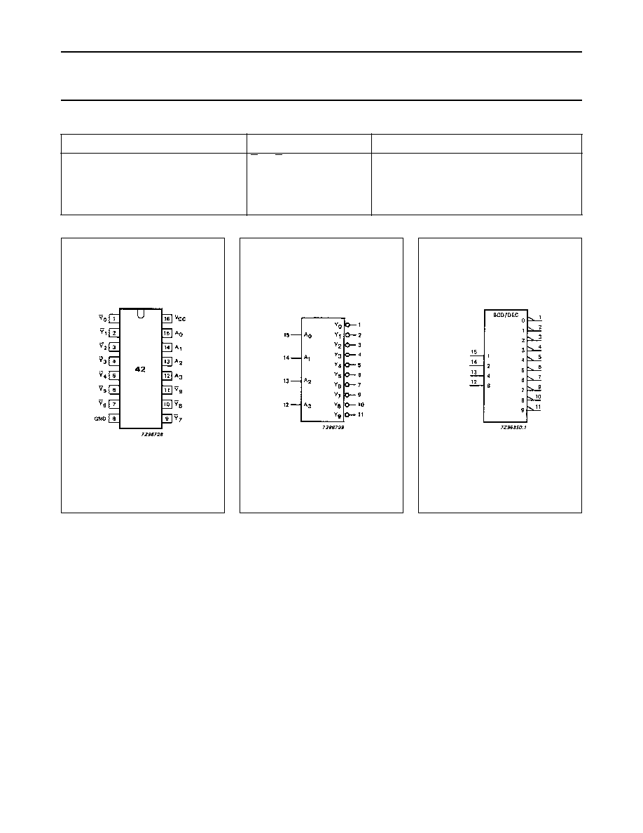
PIN DESCRIPTION
PIN NO.
SYMBOL
NAME AND FUNCTION
1, 2, 3, 4, 5, 6, 7, 9, 10, 11
Y
0
to Y
9
multiplexer outputs
8
GND
ground (0 V)
15, 14, 13, 12
A
0
to A
3
data inputs
16
V
CC
positive supply voltage
Fig.1 Pin configuration.
Fig.2 Logic symbol.
Fig.3 IEC logic symbol.
December 1990
4
Philips Semiconductors
Product specification
BCD to decimal decoder (1-of-10)
74HC/HCT42
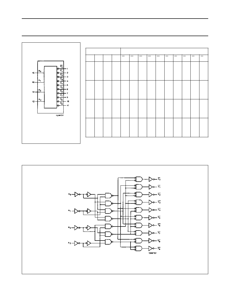
Fig.4 Functional diagram.
FUNCTION TABLE
Note
1. H = HIGH voltage level
L = LOW voltage level
INPUTS
OUTPUTS
A
3
A
2
A
1
A
0
Y
0
Y
1
Y
2
Y
3
Y
4
Y
5
Y
6
Y
7
Y
8
Y
9
L
L
L
L
L
L
L
L
L
L
H
H
L
H
L
H
L
H
H
H
H
L
H
H
H
H
L
H
H
H
H
L
H
H
H
H
H
H
H
H
H
H
H
H
H
H
H
H
H
H
H
H
H
H
H
H
L
L
L
L
H
H
H
H
L
L
H
H
L
H
L
H
H
H
H
H
H
H
H
H
H
H
H
H
H
H
H
H
L
H
H
H
H
L
H
H
H
H
L
H
H
H
H
L
H
H
H
H
H
H
H
H
H
H
H
H
L
L
L
L
L
L
H
H
L
H
L
H
H
H
H
H
H
H
H
H
H
H
H
H
H
H
H
H
H
H
H
H
H
H
H
H
H
H
H
H
H
H
H
H
L
H
H
H
H
L
H
H
H
H
H
H
H
H
H
H
L
L
H
H
L
H
L
H
H
H
H
H
H
H
H
H
H
H
H
H
H
H
H
H
H
H
H
H
H
H
H
H
H
H
H
H
H
H
H
H
H
H
H
H
H
H
H
H
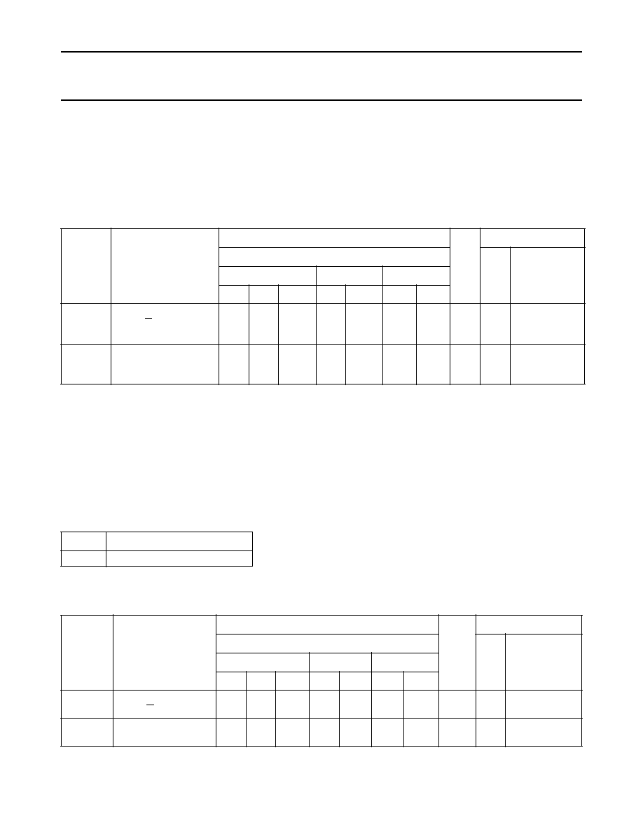
Fig.5 Logic diagram.
December 1990
5
Philips Semiconductors
Product specification
BCD to decimal decoder (1-of-10)
74HC/HCT42
DC CHARACTERISTICS FOR 74HC
For the DC characteristics see
"74HC/HCT/HCU/HCMOS Logic Family Specifications"
.
Output capability: standard
I
CC
category: MSI
AC CHARACTERISTICS FOR 74HC
GND = 0 V; t
r
= t
f
= 6 ns; C
L
= 50 pF
DC CHARACTERISTICS FOR 74HCT
For the DC characteristics see
"74HC/HCT/HCU/HCMOS Logic Family Specifications"
.
Output capability: standard
I
CC
category: MSI
Note to HCT types
The value of additional quiescent supply current (
I
CC
) for a unit load of 1 is given in the family specifications.
To determine
I
CC
per input, multiply this value by the unit load coefficient shown in the table below.
AC CHARACTERISTICS FOR 74HCT
GND = 0 V; t
r
= t
f
= 6 ns; C
L
= 50 pF
SYMBOL PARAMETER
T
amb
(
∞
C)
TEST CONDITIONS
74HC
UNIT
V
CC
(V)
WAVEFORMS
+
25
-
40 to
+
85
-
40 to
+
125
min.
typ.
max.
min.
max.
min.
max.
t
PHL
/ t
PLH
propagation delay
A
n
to Y
n
47
17
14
150
30
26
190
38
33
225
45
38
ns
2.0
4.5
6.0
Fig.6
t
THL
/ t
TLH
output transition time
19
7
6
75
15
13
95
19
16
110
22
19
ns
2.0
4.5
6.0
Fig.6
INPUT
UNIT LOAD COEFFICIENT
A
n
1.0
SYMBOL
PARAMETER
T
amb
(
∞
C)
TEST CONDITIONS
74HCT
UNIT
V
CC
(V)
WAVEFORMS
+
25
-
40 to
+
85
-
40 to
+
125
min.
typ.
max.
min.
max.
min.
max.
t
PHL
/ t
PLH
propagation delay
A
n
to Y
n
20
35
44
53
ns
4.5
Fig.6
t
THL
/ t
TLH
output transition time
7
15
19
22
ns
4.5
Fig.6
December 1990
6
Philips Semiconductors
Product specification
BCD to decimal decoder (1-of-10)
74HC/HCT42
AC WAVEFORMS
PACKAGE OUTLINES
See
"74HC/HCT/HCU/HCMOS Logic Package Outlines"
.
Fig.6
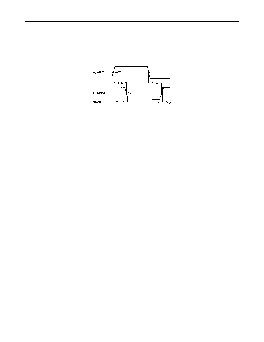
Waveforms showing the input (A
n
) to output (Y
n
) propagation delays and the output transition times.
(1) HC : V
M
= 50%; V
I
= GND to V
CC
.
HCT: V
M
= 1.3 V; V
I
= GND to 3 V.