DATA SHEET
Product specification
File under Integrated Circuits, IC06
December 1990
INTEGRATED CIRCUITS
74HC/HCT4511
BCD to 7-segment
latch/decoder/driver
For a complete data sheet, please also download:
∑
The IC06 74HC/HCT/HCU/HCMOS Logic Family Specifications
∑
The IC06 74HC/HCT/HCU/HCMOS Logic Package Information
∑
The IC06 74HC/HCT/HCU/HCMOS Logic Package Outlines

December 1990
2
Philips Semiconductors
Product specification
BCD to 7-segment latch/decoder/driver
74HC/HCT4511
FEATURES
∑
Latch storage of BCD inputs
∑
Blanking input
∑
Lamp test input
∑
Driving common cathode LED displays
∑
Guaranteed 10 mA drive capability per output
∑
Output capability: non-standard
∑
I
CC
category: MSI
GENERAL DESCRIPTION
The 74HC/HCT4511 are high-speed Si-gate CMOS
devices and are pin compatible with "4511" of the "4000B"
series. They are specified in compliance with JEDEC
standard no. 7A.
The 74HC/HCT4511 are BCD to 7-segment
latch/decoder/drivers with four address inputs (D
1
to D
4
),
an active LOW latch enable input (LE), an active LOW
ripple blanking input (BI), an active LOW lamp test input
(LT), and seven active HIGH segment outputs (Q
a
to Q
g
).
When LE is LOW, the state of the segment outputs (Q
a
to
Q
g
) is determined by the data on D
1
to D
4
.
When LE goes HIGH, the last data present on D
1
to D
4
are
stored in the latches and the segment outputs remain
stable.
When LT is LOW, all the segment outputs are HIGH
independent of all other input conditions. With LT HIGH, a
LOW on BI forces all segment outputs LOW. The inputs LT
and BI do not affect the latch circuit.
APPLICATIONS
∑
Driving LED displays
∑
Driving incandescent displays
∑
Driving fluorescent displays
∑
Driving LCD displays
∑
Driving gas discharge displays
QUICK REFERENCE DATA
GND = 0 V; T
amb
= 25
∞
C; t
r
= t
f
= 6 ns
Notes
1. C
PD
is used to determine the dynamic power dissipation (P
D
in
µ
W):
P
D
= C
PD
◊
V
CC
2
◊
f
i
+
(C
L
◊
V
CC
2
◊
f
o
) where:
f
i
= input frequency in MHz
f
o
= output frequency in MHz
(C
L
◊
V
CC
2
◊
f
o
) = sum of outputs
C
L
= output load capacitance in pF
V
CC
= supply voltage in V
2. For HC the condition is V
I
= GND to V
CC
For HCT the condition is V
I
= GND to V
CC
-
1.5 V
SYMBOL
PARAMETER
CONDITIONS
TYPICAL
UNIT
HC
HCT
t
PHL
/ t
PLH
propagation delay
C
L
= 15 pF; V
CC
= 5 V
D
n
to Q
n
24
24
ns
LE to Q
n
23
24
ns
BI to Q
n
19
20
ns
LT to Q
n
12
13
ns
C
I
input capacitance
3.5
3.5
pF
C
PD
power dissipation capacitance per latch
notes 1 and 2
64
64
pF

December 1990
3
Philips Semiconductors
Product specification
BCD to 7-segment latch/decoder/driver
74HC/HCT4511
ORDERING INFORMATION
See
"74HC/HCT/HCU/HCMOS Logic Package Information"
.
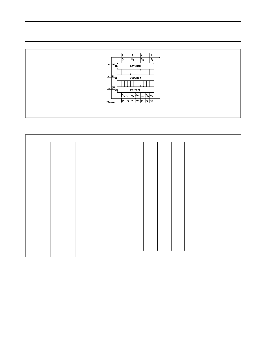
PIN DESCRIPTION
PIN NO.
SYMBOL
NAME AND FUNCTION
3
LT
lamp test input (active LOW)
4
BI
ripple blanking input (active LOW)
5
LE
latch enable input (active LOW)
7, 1, 2, 6
D
1
to D
4
BCD address inputs
8
GND
ground (0 V)
13, 12, 11, 10, 9, 15, 14
Q
a
to Q
g
segments outputs
16
V
CC
positive supply voltage
Fig.1 Pin configuration.
Fig.2 Logic symbol.
Fig.3 IEC logic symbol.
December 1990
4
Philips Semiconductors
Product specification
BCD to 7-segment latch/decoder/driver
74HC/HCT4511
FUNCTION TABLE
Note
1. Depends upon the BCD-code applied during the LOW-to-HIGH transition of LE.
H = HIGH voltage level
L = LOW voltage level
X = don't care
INPUTS
OUTPUTS
DISPLAY
LE
BI
LT
D
4
D
3
D
2
D
1
Q
a
Q
b
Q
c
Q
d
Q
e
Q
f
Q
g
X
X
L
X
X
X
X
H
H
H
H
H
H
H
8
X
L
H
X
X
X
X
L
L
L
L
L
L
L
blank
L
L
L
L
H
H
H
H
H
H
H
H
L
L
L
L
L
L
L
L
L
L
H
H
L
H
L
H
H
L
H
H
H
H
H
H
H
H
L
H
H
L
H
H
H
L
H
L
H
L
L
L
L
L
H
H
0
1
2
3
L
L
L
L
H
H
H
H
H
H
H
H
L
L
L
L
H
H
H
H
L
L
H
H
L
H
L
H
L
H
L
H
H
L
L
H
H
H
H
H
L
H
H
L
L
L
H
L
H
H
H
L
H
H
H
L
4
5
6
7
L
L
L
L
H
H
H
H
H
H
H
H
H
H
H
H
L
L
L
L
L
L
H
H
L
H
L
H
H
H
L
L
H
H
L
L
H
H
L
L
H
L
L
L
H
L
L
L
H
H
L
L
H
H
L
L
8
9
blank
blank
L
L
L
L
H
H
H
H
H
H
H
H
H
H
H
H
H
H
H
H
L
L
H
H
L
H
L
H
L
L
L
L
L
L
L
L
L
L
L
L
L
L
L
L
L
L
L
L
L
L
L
L
L
L
L
L
blank
blank
blank
blank
H
H
H
X
X
X
X
(1)
(1)
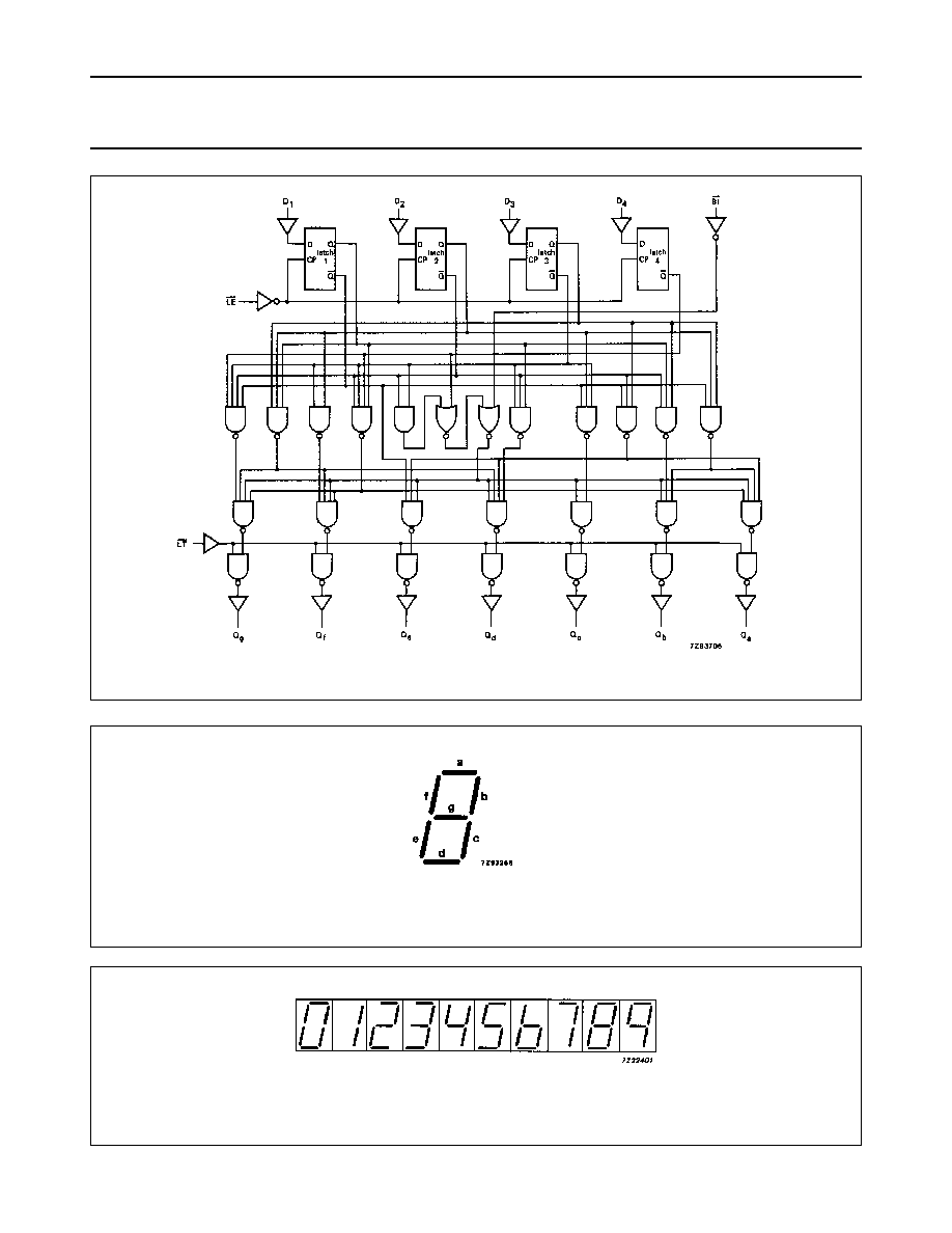
Fig.4 Functional diagram.