 | –≠–ª–µ–∫—Ç—Ä–æ–Ω–Ω—ã–π –∫–æ–º–ø–æ–Ω–µ–Ω—Ç: 74HC5555D | –°–∫–∞—á–∞—Ç—å:  PDF PDF  ZIP ZIP |

DATA SHEET
Product specification
File under Integrated Circuits, IC06
September 1993
INTEGRATED CIRCUITS
74HC/HCT5555
Programmable delay timer with
oscillator
For a complete data sheet, please also download:
∑
The IC06 74HC/HCT/HCU/HCMOS Logic Family Specifications
∑
The IC06 74HC/HCT/HCU/HCMOS Logic Package Information
∑
The IC06 74HC/HCT/HCU/HCMOS Logic Package Outlines
September 1993
2
Philips Semiconductors
Product specification
Programmable delay timer with oscillator
74HC/HCT5555
FEATURES
∑
Positive and negative edge
triggered
∑
Retriggerable or non-retriggerable
∑
Programmable delay
minimum: 100 ns
maximum: depends on input
frequency and division ratio
∑
Divide-by range of 2 to 2
24
∑
Direct reset terminates output
pulse
∑
Very low power consumption in
triggered start mode
∑
3 oscillator operating modes:
≠ RC oscillator
≠ Crystal oscillator
≠ External oscillator
∑
Device is unaffected by variations
in temperature and V
CC
when using
an external oscillator
∑
Automatic power-ON reset
∑
Schmitt trigger action on both
trigger inputs
∑
Direct drive for a power transistor
∑
Low power consumption in active
mode with respect to TTL type
timers
∑
High precision due to digital timing
∑
Output capability: 20 mA
∑
I
CC
category: MSI.
APPLICATIONS
∑
Motor control
∑
Attic fan timers
∑
Delay circuits
∑
Automotive applications
∑
Precision timing
∑
Domestic appliances.
GENERAL DESCRIPTION
The 74HC/HCT5555 are high-speed
Si-gate CMOS devices and are pin
compatible with low power Schottky
TTL (LSTTL). They are specified in
compliance with JEDEC standard
no. 7A.
The 74HC/HCT5555 are precision
programmable delay timers which
consist of:
∑
24-stage binary counter
∑
integrated oscillator (using external
timing components)
∑
retriggerable/non-retriggerable
monostable
∑
automatic power-ON reset
∑
output control logic
∑
oscillator control logic
∑
overriding asynchronous master
reset (MR).
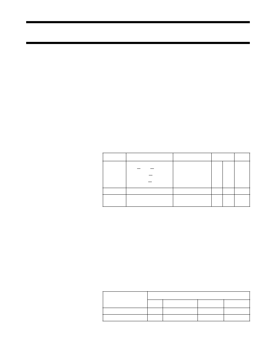
QUICK REFERENCE DATA
GND = 0 V; T
amb
= 25
∞
C; t
r
= t
f
= 6 ns.
Notes
1. C
PD
is used to determine the dynamic power dissipation (P
D
in
µ
W):
P
D
= C
PD
x V
CC
2
x f
i
+
(C
L
x V
CC
2
x f
o
) where:
f
i
= input frequency in MHz
f
o
= output frequency in MHz
(C
L
x V
CC
2
x f
o
) = sum of outputs.
C
L
= output load capacitance in pF
V
CC
= supply voltage in V
2. For HC the condition is V
I
= GND to V
CC
For HCT the condition is V
I
= GND to V
CC
-
1.5 V.
ORDERING INFORMATION
SYMBOL
PARAMETER
CONDITIONS
TYP.
UNIT
t
PHL
/t
PLH
propagation delay
C
L
= 15 pF;
V
CC
= 5 V
A, B to Q/Q
24
24
ns
MR to Q/Q
19
20
ns
RS to Q/Q
26
28
ns
C
I
input capacitance
3.5
3.5
pF
C
PD
power dissipation
capacitance per buffer
notes 1 and 2
23
36
pF
EXTENDED TYPE
NUMBER
PACKAGE
PINS
PIN POSITION
MATERIAL
CODE
74HC/HCT5555N
16
DIL
plastic
SOT38Z
74HC/HCT5555D
16
SO16
plastic
SOT109A

September 1993
3
Philips Semiconductors
Product specification
Programmable delay timer with oscillator
74HC/HCT5555
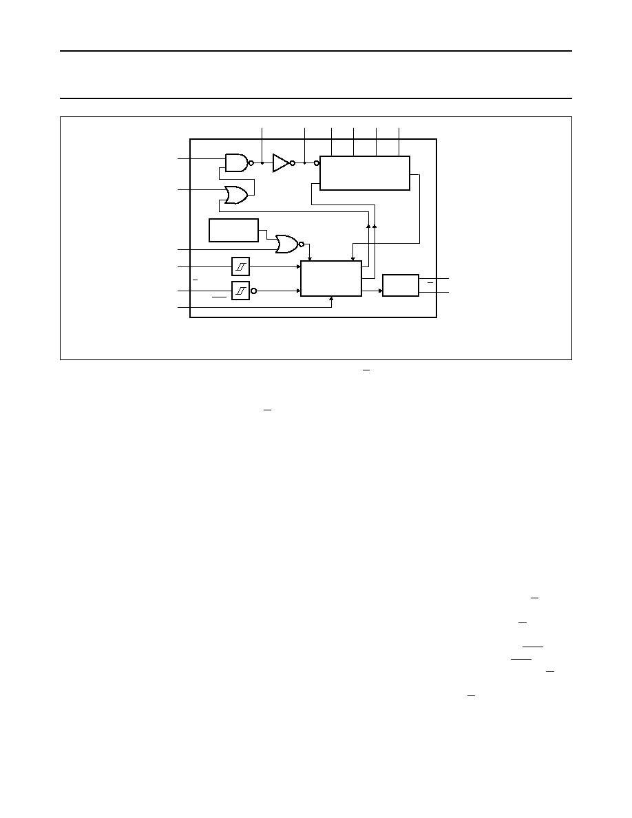
PINNING
SYMBOL
PIN
DESCRIPTION
RS
1
clock input/oscillator pin
R
TC
2
external resistor connection
C
TC
3
external capacitor connection
A
4
trigger input (positive-edge
triggered)
B
5
trigger input (negative-edge
triggered)
RTR/RTR
6
retriggerable/non-retriggerable
input (active HIGH/active LOW)
Q
7
pulse output (active LOW)
GND
8
ground (0 V)
Q
9
pulse output (active HIGH)
S
0
-
S
3
10, 11,
12, 13
programmable input
OSC CON
14
oscillator control
MR
15
master reset input (active
HIGH)
V
CC
16
positive supply voltage
Fig.1 Pin configuration.
handbook, halfpage
1
2
3
4
5
6
7
8
16
15
14
13
12
11
10
9
5555
GND
VCC
MGA642
R TC
C TC
Q
RS
OSC
CON
MR
A
B
RTR/
RTR
Q
0
S
1
S
2
S
S3
Fig.2 IEC logic diagram.
handbook, halfpage
MGA643
1
I = 0
S
R
R
&
CT = 0
CT = m
R
V16
7
9
17
16G17
CX
RX
1
2
4
8
X / Y
CTRDIVm
[T]
Y = 0
Y = 15
! G
+
0
15
10
11
12
13
2
3
14
1
6
4
5
15
September 1993
4
Philips Semiconductors
Product specification
Programmable delay timer with oscillator
74HC/HCT5555
Fig.3 Functional diagram.
handbook, full pagewidth
MGA644
R TC
C TC
MONOSTABLE
CIRCUITRY
Q
RS
OSC
CON
MR
A
B
1
14
15
4
5
6
9
7
2
3
10
11
12
13
POWER-ON
RESET
RTR/RTR
OUTPUT
STAGE
Q
24 - STAGE COUNTER
CP
CD
0
1
2
S
S
S
S3
FUNCTIONAL DESCRIPTION
The oscillator configuration allows the
design of RC or crystal oscillator
circuits. The device can operate from
an external clock signal applied to the
RS input (R
TC
and C
TC
must not be
connected). The oscillator frequency
is determined by the external timing
components (R
T
and C
T
), within the
frequency range 1 Hz to 4 MHz
(32 kHz to 20 MHz with crystal
oscillator).
In the HCT version the MR input is
TTL compatible but the RS input has
CMOS input switching levels. The RS
input can be driven by TTL input
levels if RS is tied to V
CC
via a pull-up
resistor.
The counter divides the frequency to
obtain a long pulse duration. The
24-stage is digitally programmed via
the select inputs (S
0
to S
3
). Pin S
3
can
also be used to select the test mode,
which is a convenient way of
functionally testing the counter.
The "5555" is triggered on either the
positive-edge, negative-edge or both.
∑
Trigger pulse applied to input A for
positive-edge triggering
∑
Trigger pulse applied input B for
negative-edge triggering
∑
Trigger pulse applied to inputs A
and B (tied together) for both
positive-edge and negative
triggering.
The Schmitt trigger action in the
trigger inputs, transforms slowly
changing input signals into sharply
defined jitter-free output signals and
provides the circuit with excellent
noise immunity.
The OSC CON input is used to select
the oscillator mode, either
continuously running (OSC CON =
HIGH) or triggered start mode (OSC
CON = LOW). The continuously
running mode is selected where a
start-up delay is an undesirable
feature and the triggered start mode
is selected where very low power
consumption is the primary concern.
The start of the programmed time
delay occurs when output Q goes
HIGH (in the triggered start mode, the
previously disabled oscillator will
start-up). After the programmed time
delay, the flip-flop stages are reset
and the output returns to its original
state.
An internal power-on reset is used to
reset all flip-flop stages.
The output pulse can be terminated
by the asynchronous overriding
master reset (MR), this results in all
flip-flop stages being reset. The
output signal is capable of driving a
power transistor. The output time
delay is calculated using the following
formula (minimum time delay is
100 ns):
Once triggered, the output width may
be extended by retriggering the
gated, active HIGH-going input A or
the active LOW-going input B. By
repeating this process, the output
pulse period (Q = HIGH, Q = LOW)
can be made as long as desired. This
mode is selected by RTR/RTR =
HIGH. A LOW on RTR/RTR makes,
once triggered, the outputs (Q, Q)
independent of further transitions of
inputs A and B.
1
f
i
---
division ratio (s).
◊
September 1993
5
Philips Semiconductors
Product specification
Programmable delay timer with oscillator
74HC/HCT5555
ndbook, full pagewidth
MGA655
R
TC
C
TC
Q
RS
OSC
CON
MR
A
B
RTR
/
RTR
Q
0
S
1
S
2
S
S
3
CP
CD
Q
CP
CD
Q
CP
CD
Q
CP
CD
Q
CP
CD
Q
CP
CD
Q
CP
CD
Q
CP
CD
Q
CP
CD
Q
CP
CD
Q
CP
CD
Q
CP
CD
Q
CP
CD
Q
CP
CD
Q
CP
CD
Q
CP
CD
Q
CP
CD
Q
CP
CD
Q
CP
CD
Q
CP
CD
Q
CP
CD
Q
CP
CD
Q
CP
CD
Q
CP
CD
Q
CP
CD
Q
V
CC
Fig.4 Logic diagram.