
1.
General description
The 74HC590 is a high-speed Si-gate CMOS device and is pin compatible with Low
power Schottky TTL (LSTTL). It is specified in compliance with JEDEC standard no. 7A.
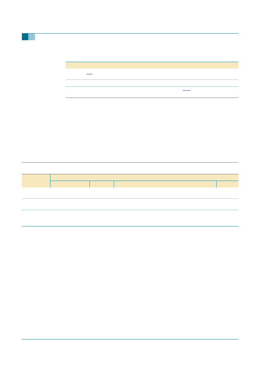
The 74HC590 is an 8-bit binary counter with a storage register and 3-state outputs. The
storage register has parallel (Q0 to Q7) outputs. The binary counter features a master
reset counter (MRC) and count enable (CE) inputs. The counter and storage register have
separate positive edge triggered clock (CPC and CPR) inputs. If both clocks are
connected together, the counter state always is one count ahead of the register. Internal
circuitry prevents clocking from the clock enable. A ripple carry output (RCO) is provided
for cascading. Cascading is accomplished by connecting RCO of the first stage to CE of
the second stage. Cascading for larger count chains can be accomplished by connecting
RCO of each stage to the counter clock (CPC) input of the following stage. If both clocks
are connected together, the counter state always is one count ahead of the register.
2.
Features
s
Counter and register have independent clock inputs
s
Counter has master reset
s
Complies with JEDEC standard no. 7A
s
Multiple package options
s
ESD protection:
x
HBM EIA/JESD22-A114-B exceeds 2000 V
x
MM EIA/JESD22-A115-A exceeds 200 V
x
CDM EIA/JESD22-C101C exceeds 2000 V
s
Specified from
-
40
�
C to +80
�
C and from
-
40
�
C to +125
�
C
3.
Quick reference data
74HC590
8-bit binary counter with output register; 3-state
Rev. 01 -- 30 March 2005
Product data sheet
Table 1:
Quick reference data
GND = 0 V; T
amb
= 25
�
C; t
r
= t
f
= 6 ns
Symbol
Parameter
Conditions
Min
Typ
Max Unit
t
PHL
, t
PLH
propagation delay CPC to
RCO
C
L
= 50 pF; V
CC
= 4.5 V
-
19
-
ns
propagation delay CPR to
Qn
C
L
= 50 pF; V
CC
= 4.5 V
-
17
-
ns
t
PLH
propagation delay MRC to
RCO
C
L
= 50 pF; V
CC
= 4.5 V
-
18
-
ns
t
PZH
, t
PZL
3-state output enable time
OE to Qn
C
L
= 50 pF; V
CC
= 4.5 V
-
13
-
ns
9397 750 14691
� Koninklijke Philips Electronics N.V. 2005. All rights reserved.
Product data sheet
Rev. 01 -- 30 March 2005
2 of 25
Philips Semiconductors
74HC590
8-bit binary counter with output register; 3-state
[1]
C
PD
is used to determine the dynamic power dissipation (P
D
in
�
W):
P
D
= C
PD
�
V
CC
2
�
f
i
�
N +
(C
L
�
V
CC
2
�
f
o
) where:
f
i
= input frequency in MHz;
f
o
= output frequency in MHz;
C
L
= output load capacitance in pF;
V
CC
= supply voltage in V;
N = number of inputs switching;
(C
L
�
V
CC
2
�
f
o
) = sum of outputs.
[2]
The condition is V
I
= GND to V
CC
.
4.
Ordering information
t
PHZ
, t
PLZ
3-state output disable time
OE to Qn
C
L
= 50 pF; V
CC
= 4.5 V
-
13
-
ns
C
I
input capacitance
-
3.5
-
pF
C
PD
power dissipation
capacitance
[1] [2]
-
44
-
pF
Table 1:
Quick reference data
...continued
GND = 0 V; T
amb
= 25
�
C; t
r
= t
f
= 6 ns
Symbol
Parameter
Conditions
Min
Typ
Max Unit
Table 2:
Ordering information
Type number
Package
Temperature range
Name
Description
Version
74HC590D
-
40
�
C to +125
�
C
SO16
plastic small outline package; 16 leads; body width
3.9 mm
SOT109-1
74HC590PW
-
40
�
C to +125
�
C
TSSOP16
plastic thin shrink small outline package; 16 leads; body
width 4.4 mm
SOT403-1
74HC590BQ
-
40
�
C to +125
�
C
DHVQFN16 plastic dual-in-line compatible thermal enhanced very thin
quad flat package; no leads; 16 terminals; body
2.5
�
3.5
�
0.85 mm
SOT763-1
9397 750 14691
� Koninklijke Philips Electronics N.V. 2005. All rights reserved.
Product data sheet
Rev. 01 -- 30 March 2005
3 of 25
Philips Semiconductors
74HC590
8-bit binary counter with output register; 3-state
5.
Functional diagram
Fig 1.
Functional diagram
001aac542
CPR
CE
CPC
MRC
8-BIT BINARY COUNTER
8-BIT STORAGE REGISTER
12
11
10
13
OE
3-STATE OUTPUTS
Q1
Q2
Q3
Q5
Q6
Q7
Q4
Q0
15
1
2
3
4
5
6
7
14
9
RCO
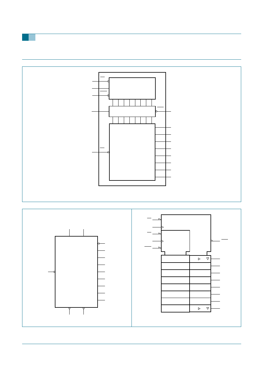
Fig 2.
Logic symbol
Fig 3.
IEC logic symbol
001aac544
RCO
OE
MRC
CPC
CE
CPR
Q0
Q1
Q2
Q3
Q4
Q5
Q6
Q7
9
11
13
12
14
10
15
1
2
3
4
5
6
7
001aac545
11
12
G1
1D
2D
15
10
CT=0
1
2
3
3
4
5
6
7
Q0
CPC
CPR
9
RCO
Q1
Q2
Q3
Q4
Q5
Q6
Q7
1
+
13
14
EN3
C2
2D
3
CTR8
(CT=255)Z4
MRC
CE
OE
9397 750 14691
� Koninklijke Philips Electronics N.V. 2005. All rights reserved.
Product data sheet
Rev. 01 -- 30 March 2005
4 of 25
Philips Semiconductors
74HC590
8-bit binary counter with output register; 3-state
Fig 4.
Logic diagram
T
R
1R
C1
1S
15
Q0
9
RCO
T
R
1R
C1
1S
1
Q1
T
R
1R
C1
1S
2
Q2
T
R
1R
C1
1S
3
Q3
T
R
1R
C1
1S
4
Q4
T
R
1R
C1
1S
5
Q5
T
R
1R
C1
1S
6
Q6
T
R
1R
C1
1S
7
Q7
14
13
12
11
10
MRC
CPC
CE
CPR
OE
001aac543
9397 750 14691
� Koninklijke Philips Electronics N.V. 2005. All rights reserved.
Product data sheet
Rev. 01 -- 30 March 2005
5 of 25
Philips Semiconductors
74HC590
8-bit binary counter with output register; 3-state
6.
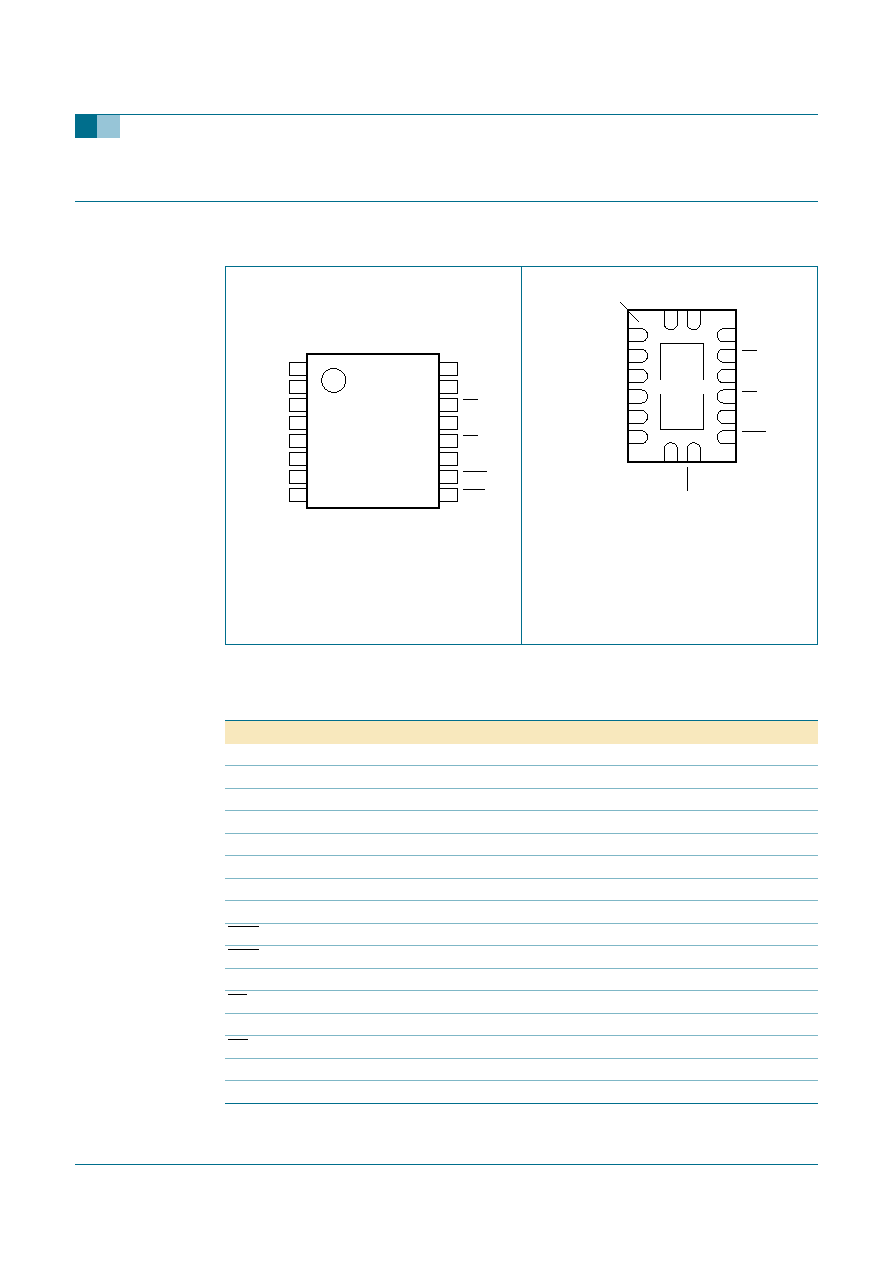
Pinning information
6.1 Pinning
6.2 Pin description
(1) The die substrate is attached to the
exposed die pad using conductive die
attach material. It can not be used as
a supply pin or input.
Fig 5.
Pin configuration SO16 and
TSSOP16
Fig 6.
Pin configuration DHVQFN16
74HC590
Q1
V
CC
Q2
Q0
Q3
OE
Q4
CPR
Q5
CE
Q6
CPC
Q7
MRC
GND
RCO
001aac564
1
2
3
4
5
6
7
8
10
9
12
11
14
13
16
15
001aac547
74HC590
Q7
MRC
Q6
CPC
GND
(1)
Q5
CE
Q4
CPR
Q3
OE
Q2
Q0
GND
RCO
Q1
V
CC
Transparent top view
7
10
6
11
5
12
4
13
3
14
2
15
8
9
1
16
terminal 1
index area
Table 3:
Pin description
Symbol
Pin
Description
Q1
1
parallel data output 1
Q2
2
parallel data output 2
Q3
3
parallel data output 3
Q4
4
parallel data output 4
Q5
5
parallel data output 5
Q6
6
parallel data output 6
Q7
7
parallel data output 7
GND
8
ground (0 V)
RCO
9
ripple carry output (active LOW)
MRC
10
master reset counter input (active LOW)
CPC
11
counter clock input (active HIGH)
CE
12
count enable input (active LOW)
CPR
13
register clock input (active HIGH)
OE
14
output enable input (active LOW)
Q0
15
parallel data output 0
V
CC
16
supply voltage