2003 Jun 25
2
Philips Semiconductors
Product specification
8-bit serial-in, serial or parallel-out shift
register with output latches; 3-state
74HC595; 74HCT595
FEATURES
∑
8-bit serial input
∑
8-bit serial or parallel output
∑
Storage register with 3-state outputs
∑
Shift register with direct clear
∑
100 MHz (typical) shift out frequency
∑
ESD protection:
HBM EIA/JESD22-A114-A exceeds 2000 V
MM EIA/JESD22-A115-A exceeds 200 V.
APPLICATIONS
∑
Serial-to-parallel data conversion
∑
Remote control holding register.
DESCRIPTION
The 74HC/HCT595 are high-speed Si-gate CMOS devices
and are pin compatible with low power Schottky TTL
(LSTTL). They are specified in compliance with JEDEC
standard no. 7A.
The 74HC/HCT595 is an 8-stage serial shift register with a
storage register and 3-state outputs. The shift register and
storage register have separate clocks.
Data is shifted on the positive-going transitions of the
SH_CP input. The data in each register is transferred to
the storage register on a positive-going transition of the
ST_CP input. If both clocks are connected together, the
shift register will always be one clock pulse ahead of the
storage register.
The shift register has a serial input (DS) and a serial
standard output (Q7') for cascading. It is also provided
with asynchronous reset (active LOW) for all 8 shift
register stages. The storage register has 8 parallel 3-state
bus driver outputs. Data in the storage register appears at
the output whenever the output enable input (OE) is LOW.
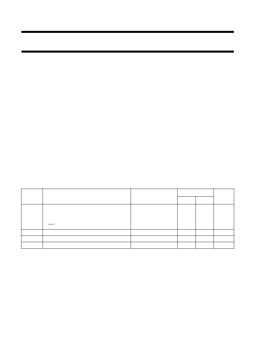
QUICK REFERENCE DATA
GND = 0 V; T
amb
= 25
∞
C; t
r
= t
f
= 6 ns.
Notes
1. C
PD
is used to determine the dynamic power dissipation (P
D
in
µ
W).
P
D
= C
PD
◊
V
CC
2
◊
f
i
◊
N +
(C
L
◊
V
CC
2
◊
f
o
) where:
f
i
= input frequency in MHz;
f
o
= output frequency in MHz;
C
L
= output load capacitance in pF;
V
CC
= supply voltage in Volts;
N = total load switching outputs;
(C
L
◊
V
CC
2
◊
f
o
) = sum of the outputs.
2. For 74HC595 the condition is V
I
= GND to V
CC
.
For 74HCT595 the condition is V
I
= GND to V
CC
-
1.5 V.
SYMBOL
PARAMETER
CONDITIONS
TYPICAL
UNIT
74HC
74HCT
t
PHL
/t
PLH
propagation delay
C
L
= 50 pF; V
CC
= 4.5 V
SH_CP to Q7'
19
25
ns
SH_CP to Qn
20
24
ns
MR to Q7'
100
52
ns
f
max
maximum clock frequency SH_CP and ST_CP
100
57
MHz
C
I
input capacitance
3.5
3.5
pF
C
PD
power dissipation capacitance per package
notes 1 and 2
115
130
pF
2003 Jun 25
3
Philips Semiconductors
Product specification
8-bit serial-in, serial or parallel-out shift
register with output latches; 3-state
74HC595; 74HCT595
FUNCTION TABLE
See note 1.
Note
1. H = HIGH voltage level;
L = LOW voltage level;
= LOW-to-HIGH transition;
= HIGH-to-LOW transition;
Z = high-impedance OFF-state;
n.c. = no change;
X = don't care.
ORDERING INFORMATION
INPUT
OUTPUT
FUNCTION
SH_CP ST_CP
OE
MR
DS
Q7'
Qn
X
X
L
L
X
L
n.c.
a LOW level on MR only affects the shift registers
X
L
L
X
L
L
empty shift register loaded into storage register
X
X
H
L
X
L
Z
shift register clear; parallel outputs in high-impedance
OFF-state
X
L
H
H
Q6'
n.c.
logic high level shifted into shift register stage 0;
contents of all shift register stages shifted through, e.g.
previous state of stage 6 (internal Q6') appears on the
serial output (Q7')
X
L
H
X
n.c.
Qn'
contents of shift register stages (internal Qn') are
transferred to the storage register and parallel output
stages
L
H
X
Q6'
Qn'
contents of shift register shifted through; previous
contents of the shift register is transferred to the
storage register and the parallel output stages
TYPE NUMBER
PACKAGE
TEMPERATURE
RANGE
PINS
PACKAGE
MATERIAL
CODE
74HC595N
-
40 to +125
∞
C
16
DIP16
plastic
SOT38-4
74HCT595N
-
40 to +125
∞
C
16
DIP16
plastic
SOT38-4
74HC595D
-
40 to +125
∞
C
16
SO16
plastic
SOT109-1
74HCT595D
-
40 to +125
∞
C
16
SO16
plastic
SOT109-1
74HC595DB
-
40 to +125
∞
C
16
SSOP16
plastic
SOT338-1
74HCT595DB
-
40 to +125
∞
C
16
SSOP16
plastic
SOT338-1
74HC595PW
-
40 to +125
∞
C
16
TSSOP16
plastic
SOT403-1
74HCT595PW
-
40 to +125
∞
C
16
TSSOP16
plastic
SOT403-1
74HC595BQ
-
40 to +125
∞
C
16
DHVQFN16
plastic
SOT763-1
74HCT595BQ
-
40 to +125
∞
C
16
DHVQFN16
plastic
SOT763-1
2003 Jun 25
4
Philips Semiconductors
Product specification
8-bit serial-in, serial or parallel-out shift
register with output latches; 3-state
74HC595; 74HCT595
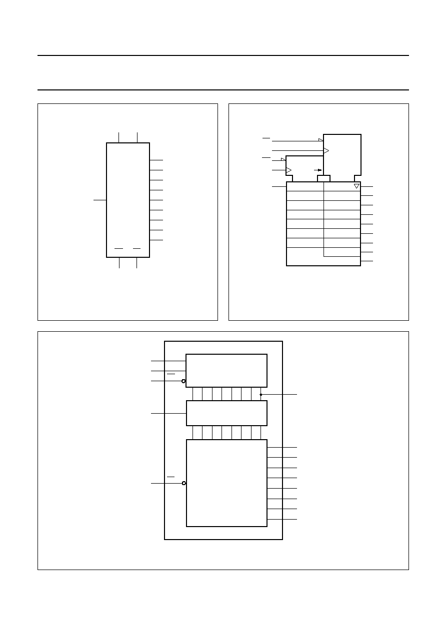
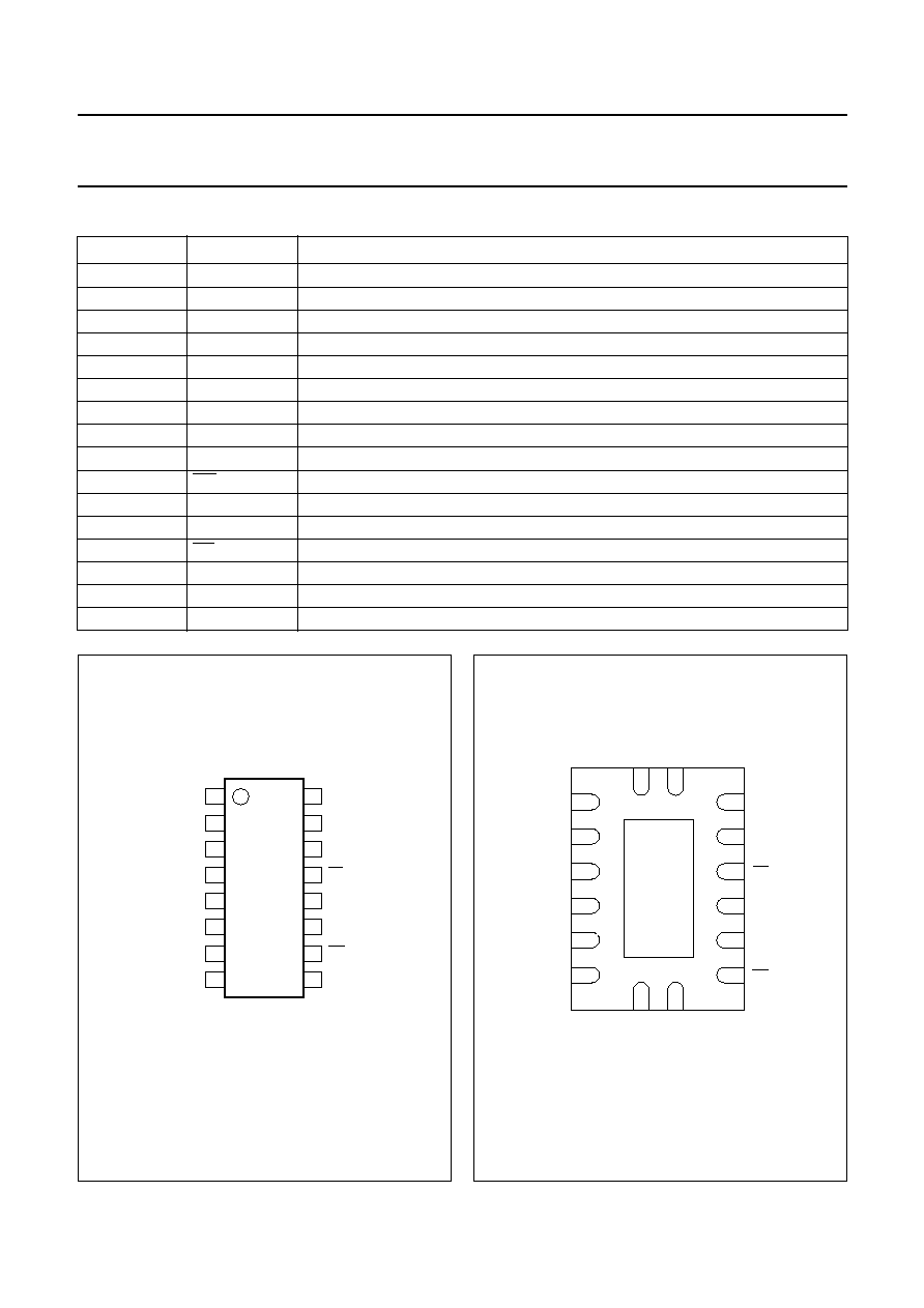
PINNING
PIN
SYMBOL
DESCRIPTION
1
Q1
parallel data output
2
Q2
parallel data output
3
Q3
parallel data output
4
Q4
parallel data output
5
Q5
parallel data output
6
Q6
parallel data output
7
Q7
parallel data output
8
GND
ground (0 V)
9
Q7'
serial data output
10
MR
master reset (active LOW)
11
SH_CP
shift register clock input
12
ST_CP
storage register clock input
13
OE
output enable (active LOW)
14
DS
serial data input
15
Q0
parallel data output
16
V
CC
positive supply voltage
handbook, halfpage
Q1
Q2
Q3
Q4
Q5
Q6
Q7
Q7'
Q0
DS
GND
ST_CP
SH_CP
VCC
OE
1
2
3
4
5
6
7
8
16
15
14
13
12
11
10
9
595
MLA001
MR
Fig.1
Pin configuration DIP16, SO16 and
(T)SSOP16.
handbook, halfpage
1
16
GND
(1)
Q1
VCC
8
2
3
4
5
7
Q2
Q3
Q4
Q5
Q6
15
14
13
12
10
6
11
9
GND
Top view
MBL893
Q7
Q7'
MR
SH_CP
ST_CP
OE
DS
Q0
Fig.2 Pin configuration DHVQFN16.
(1) The die substrate is attached to this pad using conductive die
attach material. It can not be used as a supply pin or input.