 | –≠–ª–µ–∫—Ç—Ä–æ–Ω–Ω—ã–π –∫–æ–º–ø–æ–Ω–µ–Ω—Ç: 74HC646N | –°–∫–∞—á–∞—Ç—å:  PDF PDF  ZIP ZIP |

DATA SHEET
Product specification
File under Integrated Circuits, IC06
September 1993
INTEGRATED CIRCUITS
74HC/HCT646
Octal bus transceiver/register;
3-state
For a complete data sheet, please also download:
∑
The IC06 74HC/HCT/HCU/HCMOS Logic Family Specifications
∑
The IC06 74HC/HCT/HCU/HCMOS Logic Package Information
∑
The IC06 74HC/HCT/HCU/HCMOS Logic Package Outlines
September 1993
2
Philips Semiconductors
Product specification
Octal bus transceiver/register; 3-state
74HC/HCT646
FEATURES
∑
Independent register for A and B buses
∑
Multiplexed real-time and stored data
∑
Output capability: bus driver
∑
I
CC
category: MSI
GENERAL DESCRIPTION
The 74HC/HCT646 are high-speed Si-gate CMOS devices
and are pin compatible with low power Schottky TTL
(LSTTL). They are specified in compliance with JEDEC
standard no. 7A.
The 74HC/HCT646 consist of bus transceiver circuits with
3-state outputs, D-type flip-flops, and control circuitry
arranged for multiplexed transmission of data directly from
the internal registers. Data on the "A" or "B" bus will be
clocked into the registers as the appropriate clock
(CP
AB
and CP
BA
) goes to a HIGH logic level. Output
enable (OE) and direction (DIR) inputs are provided to
control the transceiver function. In the transceiver mode,
data present at the high-impedance port may be stored in
either the "A" or "B" register, or in both. The select source
inputs (S
AB
and S
BA
) can multiplex stored and real-time
(transparent mode) data. The direction (DIR) input
determines which bus will receive data when OE is active
(LOW). In the isolation mode (OE = HIGH), "A" data may
be stored in the "B" register and/or "B" data may be stored
in the "A" register.
When an output function is disabled, the input function is
still enabled and may be used to store and transmit data.
Only one of the two buses, A or B, may be driven at a time.
The "646" is functionally identical to the "648", but has
non-inverting data paths.
QUICK REFERENCE DATA
GND = 0 V; T
amb
= 25
∞
C; t
r
= t
f
= 6 ns
Notes
1. C
PD
is used to determine the dynamic power dissipation (P
D
in
µ
W):
P
D
= C
PD
◊
V
CC
2
◊
f
i
+
(C
L
◊
V
CC
2
◊
f
o
) where:
f
i
= input frequency in MHz
f
o
= output frequency in MHz
(C
L
◊
V
CC
2
◊
f
o
) = sum of outputs
C
L
= output load capacitance in pF
V
CC
= supply voltage in V
2. For HC the condition is V
I
= GND to V
CC
For HCT the condition is V
I
= GND to V
CC
-
1.5 V
ORDERING INFORMATION
See
"74HC/HCT/HCU/HCMOS Logic Package Information"
.
SYMBOL
PARAMETER
CONDITIONS
TYPICAL
UNIT
HC
HCT
t
PHL
/ t
PLH
propagation delay
A
n
, B
n
to B
n
, A
n
C
L
= 15 pF; V
CC
= 5 V
11
13
ns
f
max
maximum clock frequency
69
85
MHz
C
I
input capacitance
3.5
3.5
pF
C
PD
power dissipation capacitance per channel
notes 1 and 2
30
33
pF
September 1993
3
Philips Semiconductors
Product specification
Octal bus transceiver/register; 3-state
74HC/HCT646
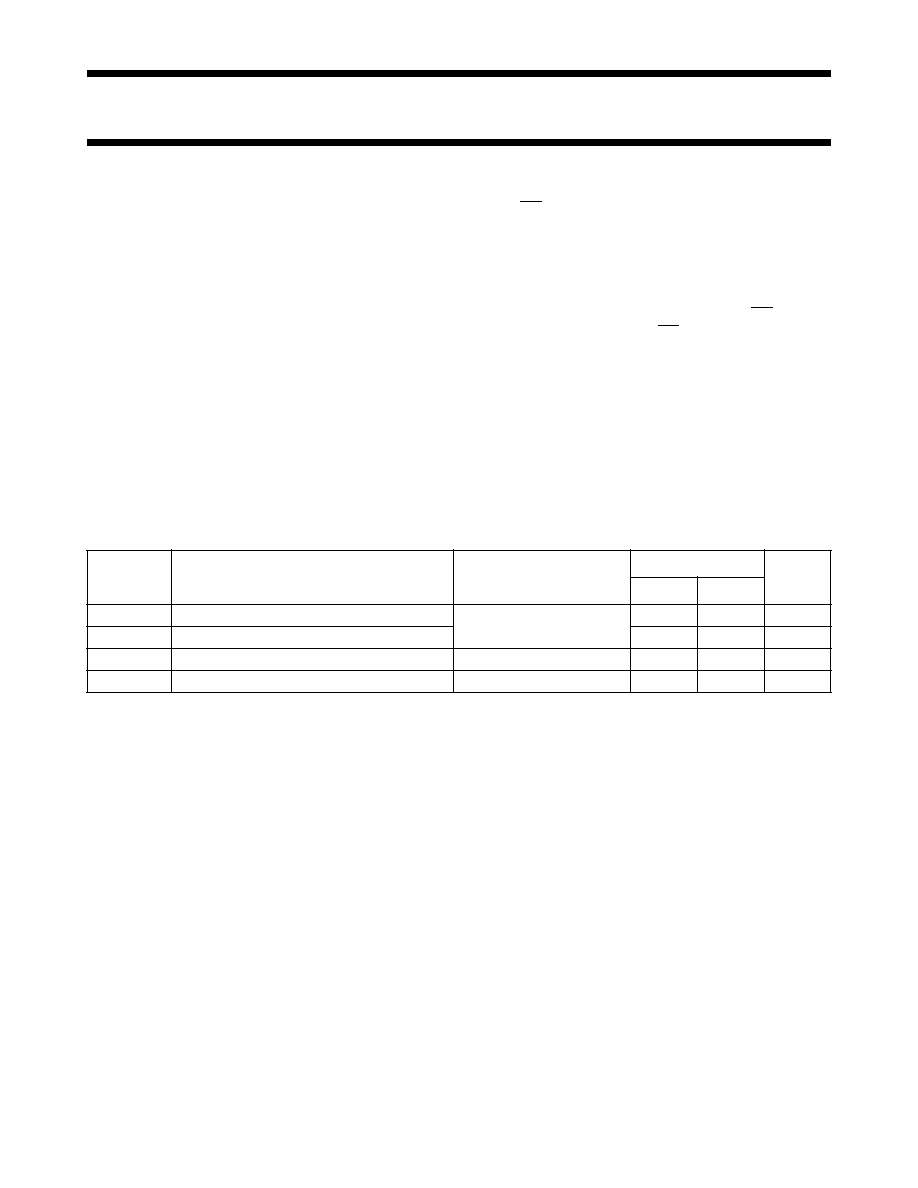
PIN DESCRIPTION
PIN NO.
SYMBOL
NAME AND FUNCTION
1
CP
AB
A to B clock input (LOW-to-HIGH, edge-triggered)
2
S
AB
select A to B source input
3
DIR
direction control input
4, 5, 6, 7, 8, 9, 10, 11
A
0
to A
7
A data inputs/outputs
12
GND
ground (0 V)
20, 19, 18, 17, 16, 15, 14, 13
B
0
to B
7
B data inputs/outputs
21
OE
output enable input (active LOW)
22
S
BA
select B to A source input
23
CP
BA
B to A clock input (LOW-to-HIGH, edge-triggered)
24
V
CC
positive supply voltage
Fig.1 Pin configuration.
Fig.2 Logic symbol.
Fig.3 IEC logic symbol.
September 1993
4
Philips Semiconductors
Product specification
Octal bus transceiver/register; 3-state
74HC/HCT646
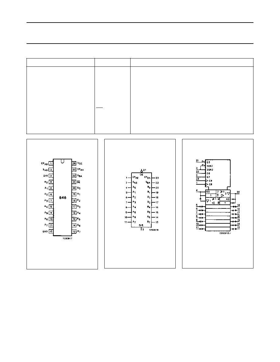
Fig.4 Functional diagram.
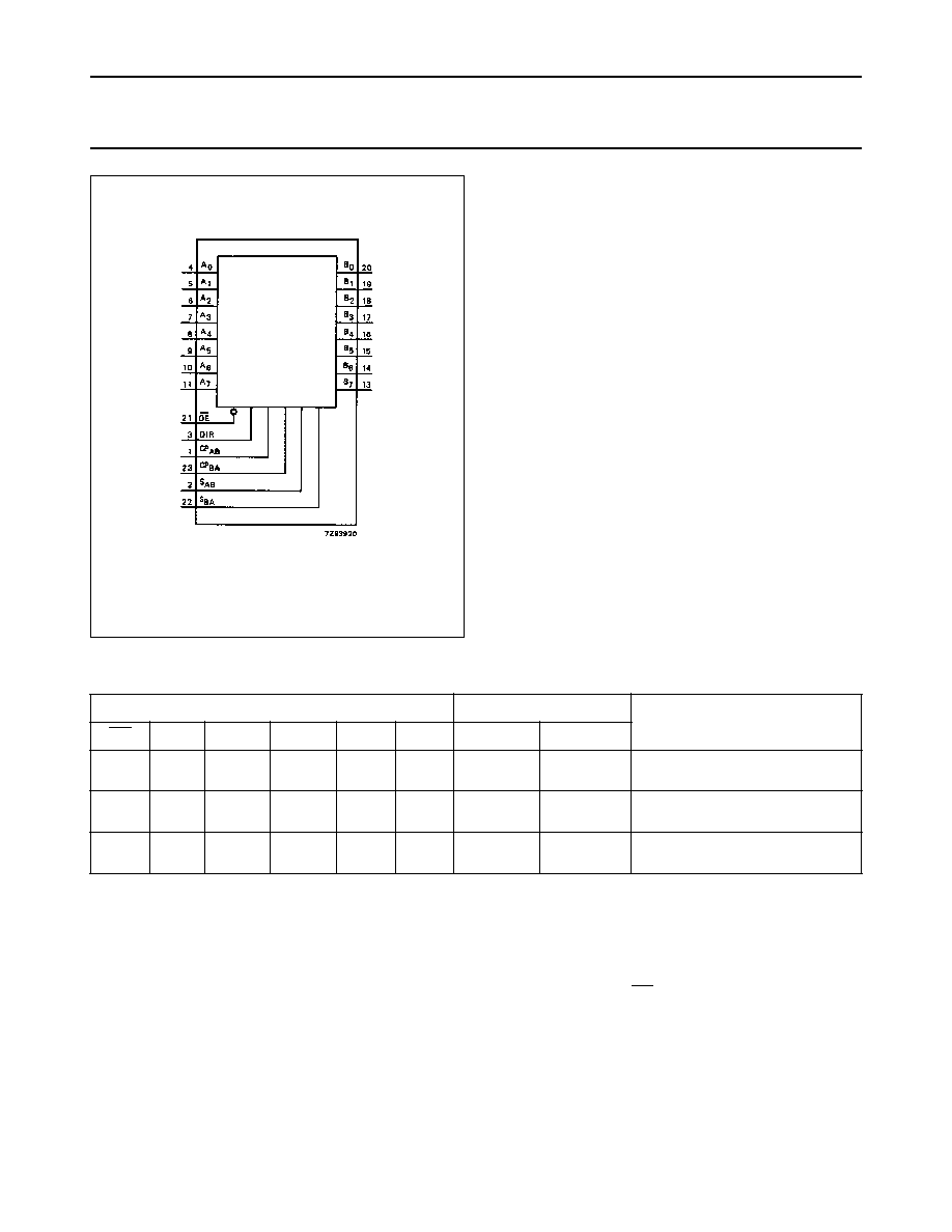
FUNCTION TABLE
Notes
1. H = HIGH voltage level
L = LOW voltage level
X = don't care
= LOW-to-HIGH level transition
2. The data output functions may be enabled or disabled by various signals at the OE and DIR inputs. Data input
functions are always enabled, i.e., data at the bus inputs will be stored on every LOW-to-HIGH transition on the clock
inputs.
INPUTS
(1)
DATA I/O
(2)
FUNCTION
OE
DIR
CP
AB
CP
BA
S
AB
S
BA
A
0
to A
7
B
0
to B
7
H
H
X
X
H or L
H or L
X
X
X
X
input
input
isolation
store A and B data
L
L
L
L
X
X
X
H or L
X
X
L
H
output
input
real-time B data to A bus
stored B data to A bus
L
L
H
H
X
H or L
X
X
L
H
X
X
input
output
real-time A data to B bus
stored A data to B bus

September 1993
5
Philips Semiconductors
Product specification
Octal bus transceiver/register; 3-state
74HC/HCT646
Fig.5 Logic diagram.
September 1993
6
Philips Semiconductors
Product specification
Octal bus transceiver/register; 3-state
74HC/HCT646
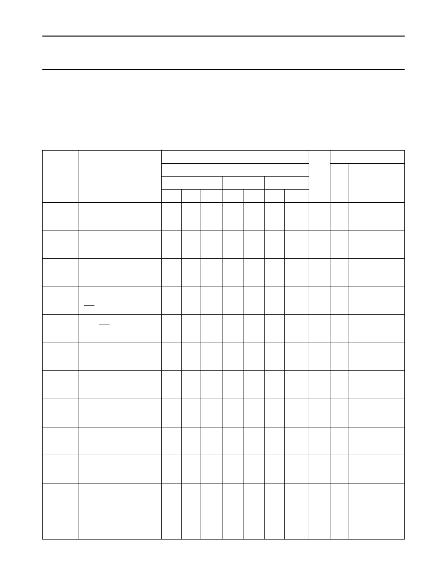
DC CHARACTERISTICS FOR 74HC
For the DC characteristics see
"74HC/HCT/HCU/HCMOS Logic Family Specifications"
.
Output capability: bus driver
I
CC
category: MSI
AC CHARACTERISTICS FOR 74HC
GND = 0 V; t
r
= t
f
= 6 ns; C
L
= 50 pF
SYMBOL
PARAMETER
T
amb
(
∞
C)
UNIT
TEST CONDITIONS
74HC
V
CC
(V)
WAVEFORMS
+25
-
40 to +85
-
40 to +125
min.
typ.
max. min. max. min.
max.
t
PHL
/ t
PLH
propagation delay
A
n
,B
n
to B
n
,A
n
39
14
11
135
27
23
170
34
29
205
41
35
ns
2.0
4.5
6.0
Fig.6
t
PHL
/ t
PLH
propagation delay
CP
AB
,CP
BA
to B
n
,A
n
66
24
19
220
44
37
275
55
47
330
66
56
ns
2.0
4.5
6.0
Fig.7
t
PHL
/ t
PLH
propagation delay
S
AB
,S
BA
to B
n
,A
n
55
20
16
190
38
32
240
48
41
285
57
48
ns
2.0
4.5
6.0
Fig.8
t
PZH
/ t
PZL
3-state output enable
time
OE to A
n
,B
n
47
17
14
175
35
30
220
44
37
265
53
45
ns
2.0
4.5
6.0
Fig.9
t
PHZ
/ t
PLZ
3-state output disable
time OE to A
n
,B
n
58
21
17
175
35
30
220
44
37
265
53
45
ns
2.0
4.5
6.0
Fig.9
t
PZH
/ t
PZL
3-state output enable
time DIR to A
n
,B
n
50
18
14
175
35
30
220
44
37
265
53
45
ns
2.0
4.5
6.0
Fig.10
t
PHZ
/ t
PLZ
3-state output disable
time DIR to A
n
,B
n
50
18
14
175
35
30
220
44
37
265
53
45
ns
2.0
4.5
6.0
Fig.10
t
THL
/ t
TLH
output transition time
14
5
4
60
12
10
75
15
13
90
18
15
ns
2.0
4.5
6.0
Fig.6 and Fig.8
t
W
clock pulse width
HIGH or LOW
CP
AB
or CP
BA
80
16
14
25
9
7
100
24
20
120
24
20
ns
2.0
4.5
6.0
Fig.7
t
su
set-up time
A
n
,B
n
to CP
AB
,CP
BA
60
12
10
-
3
-
1
-
1
75
15
13
90
18
15
ns
2.0
4.5
6.0
Fig.7
t
h
hold time
A
n
,B
n
to CP
AB
,CP
BA
35
7
6
6
2
2
45
9
8
55
11
9
ns
2.0
4.5
6.0
Fig.7
f
max
maximum clock pulse
frequency
6.0
30
35
21
63
75
4.8
24
28
4.0
20
24
MHz
2.0
4.5
6.0
Fig.7

September 1993
7
Philips Semiconductors
Product specification
Octal bus transceiver/register; 3-state
74HC/HCT646
DC CHARACTERISTICS FOR 74HCT
For the DC characteristics see
"74HC/HCT/HCU/HCMOS Logic Family Specifications"
.
Output capability: bus driver
I
CC
category: MSI
Note to HCT types
The value of additional quiescent supply current (
I
CC
) for a unit load of 1 is given in the family specifications.
To determine
I
CC
per input, multiply this value by the unit load coefficient shown in the table below.
INPUT
UNIT LOAD COEFFICIENT
S
AB
, S
BA
0.60
A
0
to A
7
and B
0
to B
7
0.75
INPUT
UNIT LOAD COEFFICIENT
CP
AB
, CP
BA
1.50
OE
DIR
1.50
1.25
September 1993
8
Philips Semiconductors
Product specification
Octal bus transceiver/register; 3-state
74HC/HCT646
AC CHARACTERISTICS FOR 74HCT
GND = 0 V; t
r
= t
f
= 6 ns; C
L
= 50 pF
SYMBOL
PARAMETER
T
amb
(
∞
C)
UNIT
TEST CONDITIONS
74HCT
V
CC
(V)
WAVEFORMS
+25
-
40 to +85
-
40 to +125
min.
typ.
max. min. max. min.
max.
t
PHL
/ t
PLH
propagation delay
A
n
,B
n
to B
n
,A
n
16
30
38
45
ns
4.5
Fig.6
t
PHL
/ t
PLH
propagation delay
CP
AB
,CP
BA
to B
n
,A
n
23
44
55
66
ns
4.5
Fig.7
t
PHL
/ t
PLH
propagation delay
S
AB
,S
BA
to B
n
,A
n
26
46
58
69
ns
4.5
Fig.8
t
PZH
/ t
PZL
3-state output enable time
OE to A
n
,B
n
21
40
50
60
ns
4.5
Fig.9
t
PHZ
/ t
PLZ
3-state output disable time
OE to A
n
,B
n
20
35
44
53
ns
4.5
Fig.9
t
PZH
/ t
PZL
3-state output enable time
DIR to A
n
,B
n
21
40
50
60
ns
4.5
Fig.10
t
PHZ
/ t
PLZ
3-state output disable time
DIR to A
n
,B
n
21
35
44
53
ns
4.5
Fig.10
t
THL
/ t
TLH
output transition time
5
12
15
18
ns
4.5
Fig.6 and Fig.8
t
W
clock pulse width
HIGH or LOW
CP
AB
or CP
BA
16
8
20
24
ns
4.5
Fig.7
t
su
set-up time
A
n
,B
n
to CP
AB
,CP
BA
12
3
15
18
ns
4.5
Fig.7
t
h
hold time
A
n
,B
n
to CP
AB
,CP
BA
5
1
5
5
ns
4.5
Fig.7
f
max
maximum clock pulse
frequency
30
77
24
20
MHz
4.5
Fig.7

September 1993
9
Philips Semiconductors
Product specification
Octal bus transceiver/register; 3-state
74HC/HCT646
AC WAVEFORMS
Fig.6 Waveforms showing the input A
n
, B
n
to output B
n
, A
n
propagation delays and the output transition times.
(1)
HC : V
M
= 50%; V
I
= GND to V
CC
.
HCT: V
M
= 1.3 V; V
I
= GND to 3 V.
Fig.7
Waveforms showing the A
n
,B
n
to CP
AB
, CP
BA
set-up and hold times, clock CP
AB
,CP
BA
pulse width,
maximum clock pulse frequency and the CP
AB
,CP
BA
to output B
n
,A
n
propagation delays.
(1)
HC : V
M
= 50%; V
I
= GND to V
CC
.
HCT: V
M
= 1.3 V; V
I
= GND to 3 V.
Fig.8 Waveforms showing the input S
AB
,S
BA
to output B
n
,A
n
propagation delays and output transition times.
(1)
HC : V
M
= 50%; V
I
= GND to V
CC
.
HCT: V
M
= 1.3 V; V
I
= GND to 3 V.
September 1993
10
Philips Semiconductors
Product specification
Octal bus transceiver/register; 3-state
74HC/HCT646
Fig.9 Waveforms showing the input OE to output A
n
,B
n
3-state enable and disable times.
(1)
HC : V
M
= 50%; V
I
= GND to V
CC
.
HCT: V
M
= 1.3 V; V
I
= GND to 3 V.
Fig.10 Waveforms showing the input DIR to output A
n
, B
n
3-state enable and disable times.
(1)
HC : V
M
= 50%; V
I
= GND to V
CC
.
HCT: V
M
= 1.3 V; V
I
= GND to 3 V.

September 1993
11
Philips Semiconductors
Product specification
Octal bus transceiver/register; 3-state
74HC/HCT646
APPLICATION INFORMATION
Fig.11 Data storage from A and/or B bus.
Fig.12 Real-time transfer from bus A to bus B.
Fig.13 Real-time transfer from bus B to bus A.

September 1993
12
Philips Semiconductors
Product specification
Octal bus transceiver/register; 3-state
74HC/HCT646
PACKAGE OUTLINES
See
"74HC/HCT/HCU/HCMOS Logic Package Outlines"
.