DATA SHEET
Product specification
File under Integrated Circuits, IC06
December 1990
INTEGRATED CIRCUITS
74HC/HCT648
Octal bus transceiver/register;
3-state; inverting
For a complete data sheet, please also download:
∑
The IC06 74HC/HCT/HCU/HCMOS Logic Family Specifications
∑
The IC06 74HC/HCT/HCU/HCMOS Logic Package Information
∑
The IC06 74HC/HCT/HCU/HCMOS Logic Package Outlines
December 1990
2
Philips Semiconductors
Product specification
Octal bus transceiver/register; 3-state;
inverting
74HC/HCT648
FEATURES
∑
Independent register for A and B buses
∑
Multiplexed real-time and stored data
∑
Output capability: bus driver
∑
I
CC
category: MSI
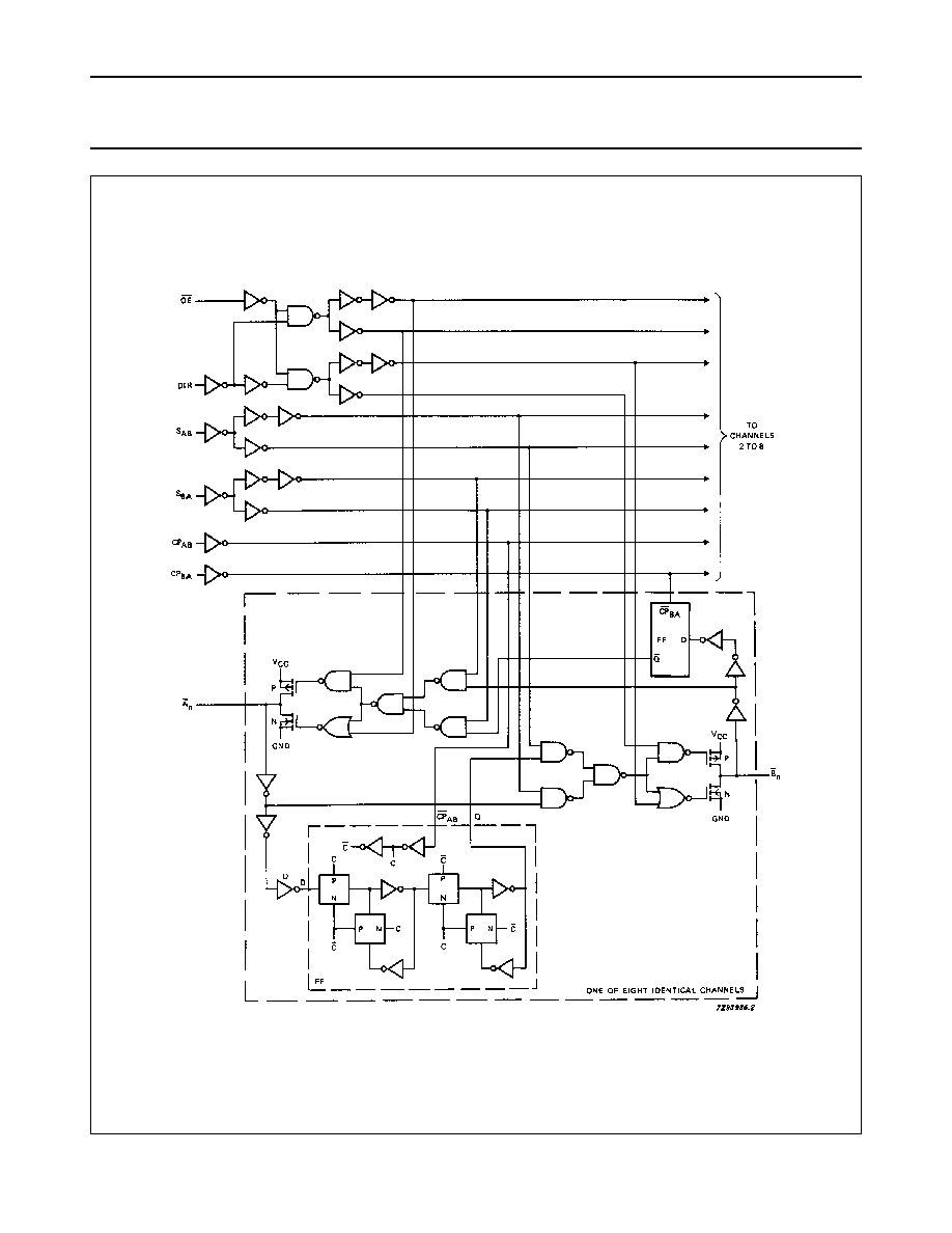
GENERAL DESCRIPTION
The 74HC/HCT648 are high-speed Si-gate CMOS devices
and are pin compatible with low power Schottky TTL
(LSTTL). They are specified in compliance with JEDEC
standard no. 7A.
The 74HC/HCT648 consist of bus transceiver circuits with
3-state inverting outputs, D-type flip-flops, and control
circuitry arranged for multiplexed transmission of data
directly from the internal registers. Data on the "A" or "B"
bus will be clocked into the registers as the appropriate
clock (CP
AB
and CP
BA
) goes to a HIGH logic level. Output
enable (OE) and direction (DIR) inputs are provided to
control the transceiver function. In the transceiver mode,
data present at the high-impedance port may be stored in
either the "A" or "B" register, or in both. The select source
inputs (S
AB
and S
BA
) can multiplex stored and real-time
(transparent mode) data. The direction (DIR) input
determines which bus will receive data when OE is active
(LOW). In the isolation mode (OE = HIGH), "A" data may
be stored in the "B" register and/or "B" data may be stored
in the "A" register.
When an output function is disabled, the input function is
still enabled and may be used to store and transmit data.
Only one of the two buses, A or B, may be driven at a time.
The "648" is functionally identical to the "646", but has
inverting data paths.
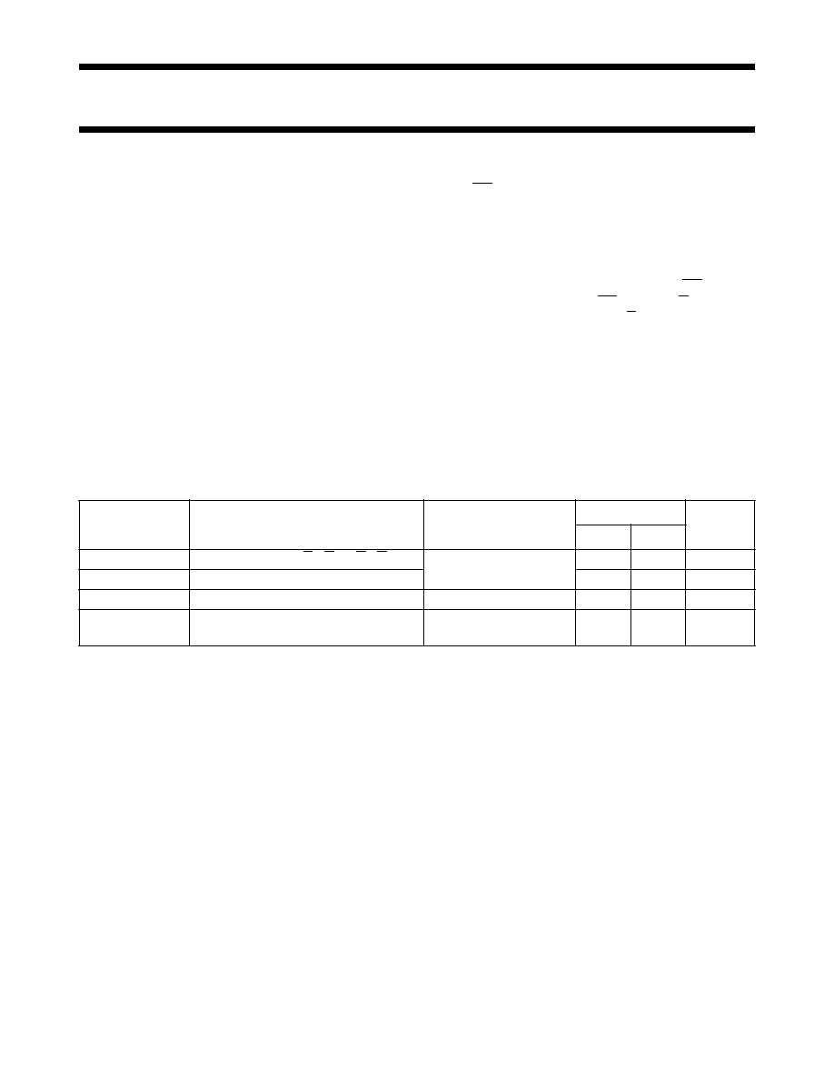
QUICK REFERENCE DATA
GND = 0 V; T
amb
= 25
∞
C; t
r
= t
f
= 6 ns
Notes
1. C
PD
is used to determine the dynamic power dissipation (P
D
in
µ
W):
P
D
= C
PD
◊
V
CC
2
◊
f
i
+
(C
L
◊
V
CC
2
◊
f
o
) where:
f
i
= input frequency in MHz
f
o
= output frequency in MHz
(C
L
◊
V
CC
2
◊
f
o
) = sum of outputs
C
L
= output load capacitance in pF
V
CC
= supply voltage in V
2. For HC the condition is V
I
= GND to V
CC
For HCT the condition is V
I
= GND to V
CC
-
1.5 V
ORDERING INFORMATION
See
"74HC/HCT/HCU/HCMOS Logic Package Information"
.
SYMBOL
PARAMETER
CONDITIONS
TYPICAL
UNIT
HC
HCT
t
PHL/
t
PLH
propagation delay A
n
, B
n
to B
n
, A
n
C
L
= 15 pF; V
CC
= 5 V
11
11
ns
f
max
maximum clock frequency
75
88
MHz
C
I
input capacitance
3.5
3.5
pF
C
PD
power dissipation capacitance per
channel
notes 1 and 2
30
31
pF
December 1990
3
Philips Semiconductors
Product specification
Octal bus transceiver/register; 3-state;
inverting
74HC/HCT648
PIN DESCRIPTION
PIN NO.
SYMBOL
NAME AND FUNCTION
1
CP
AB
A to B clock input (LOW-to-HIGH, edge-triggered)
2
S
AB
select A to B source input
3
DIR
direction control input
4, 5, 6, 7, 8, 9, 10, 11
A
0
to A
7
A data inputs/outputs
12
GND
ground (0 V)
20, 19, 18, 17, 16, 15, 14, 13
B
0
to B
7
B data inputs/outputs
21
OE
output enable input (active LOW)
22
S
BA
select B to A source input
23
CP
BA
B to A clock input (LOW-to-HIGH, edge-triggered)
24
V
CC
positive supply voltage
Fig.1 Pin configuration.
Fig.2 Logic symbol.
Fig.3 IEC logic symbol.
December 1990
4
Philips Semiconductors
Product specification
Octal bus transceiver/register; 3-state;
inverting
74HC/HCT648
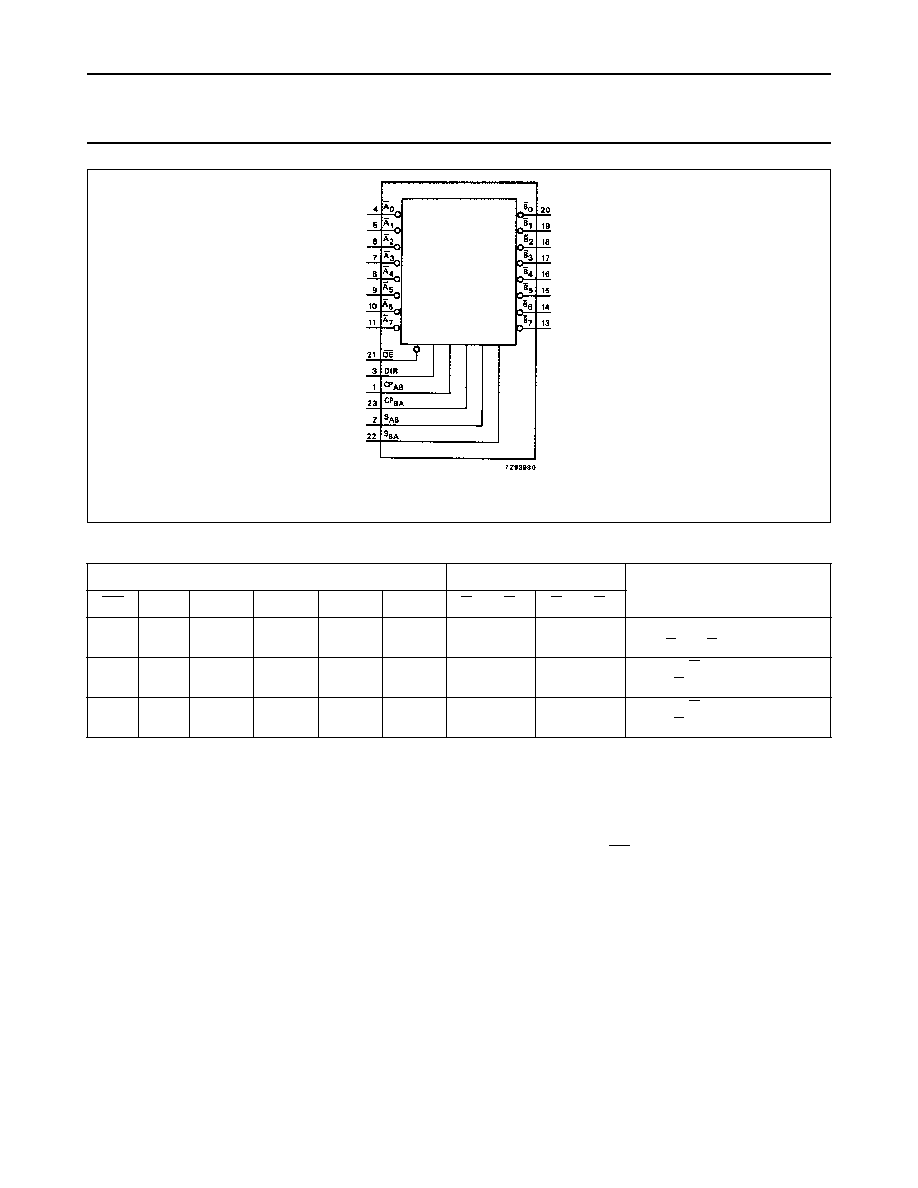
FUNCTION TABLE
Notes
1. H = HIGH voltage level
L = LOW voltage level
X = don't care
= LOW-to-HIGH level transition
2. The data output functions may be enabled or disabled by various signals at the OE and DIR inputs. Data input
functions are always enabled, i.e., data at the bus inputs will be stored on every LOW-to-HIGH transition on the clock
inputs.
INPUTS
(1)
DATA I/O
(2)
FUNCTION
OE
DIR
CP
AB
CP
BA
S
AB
S
BA
A
0
TO A
7
B
0
TO B
7
H
H
X
X
H or L
H or L
X
X
X
X
input
input
isolation
store A and B data
L
L
L
L
X
X
X
H or L
X
X
L
H
output
input
real-time B data to A bus
stored B data to A bus
L
L
H
H
X
H or L
X
X
L
H
X
X
input
output
real-time A data to B bus
stored A data to B bus
Fig.4 Functional diagram.