 | –≠–ª–µ–∫—Ç—Ä–æ–Ω–Ω—ã–π –∫–æ–º–ø–æ–Ω–µ–Ω—Ç: 74HC652N | –°–∫–∞—á–∞—Ç—å:  PDF PDF  ZIP ZIP |

DATA SHEET
Product specification
File under Integrated Circuits, IC06
September 1993
INTEGRATED CIRCUITS
74HC/HCT652
Octal bus transceiver/register;
3-state
For a complete data sheet, please also download:
∑
The IC06 74HC/HCT/HCU/HCMOS Logic Family Specifications
∑
The IC06 74HC/HCT/HCU/HCMOS Logic Package Information
∑
The IC06 74HC/HCT/HCU/HCMOS Logic Package Outlines
September 1993
2
Philips Semiconductors
Product specification
Octal bus transceiver/register; 3-state
74HC/HCT652
FEATURES
∑
Multiplexed real-time and stored
data
∑
Independent register for A and B
buses
∑
Independent enables for A and B
buses
∑
3-state
∑
Output capability: Bus driver
∑
Low power consumption by CMOS
technology
∑
I
CC
category: MSI.
APPLICATIONS
∑
Bus interfaces.
DESCRIPTION
The 74HC/HCT652 are high-speed
SI-gate CMOS devices and are pin
compatible with Low power Schottky
TTL (LSTTL). They are specified in
compliance with Jedec standard
no. 7A.
The 74HC/HCT652 consist of 8
non-inverting bus transceiver circuits
with 3-state outputs, D-type flip-flops
and central circuitry arranged for
multiplexed transmission of data
directly from the data bus or from the
internal storage registers. Data on the
"A" or "B" or both buses, will be stored
in the internal registers, at the
appropriate clock pins (CP
AB
or
CP
BA
) regardless of the select pins
(S
AB
and S
BA
) or output enable (OE
AB
and OE
BA
) control pins. Depending
on the select inputs S
AB
and S
BA
data
can directly go from input to output
(real time mode) or data can be
controlled by the clock (storage
mode), this is when the output enable
pins this operating mode permits. The
output enable pins OE
AB
and OE
BA
determine the operation mode of the
transceiver. When OE
AB
is LOW, no
data transmission from A
n
to B
n
is
possible and when OE
BA
is HIGH,
there is no data transmission from B
n
to A
n
possible. When S
AB
and S
BA
are
in the real time transfer mode, it is
also possible to store data without
using the internal D-type flip-flops by
simultaneously enabling OE
AB
and
OE
BA
. In this configuration each
output reinforces its input. Thus when
all other data sources to the two sets
of bus lines are at high-impedance,
each set of the bus lines will remain at
its last state. This type differs from the
HC/HCT646 in one extra
bus-management function. This is the
possibility to transfer stored "A data to
the "B" bus and transfer stored "B"
data to the "A" bus at the same time.
The examples at the application
information demonstrate all bus
management functions.
Schmitt-trigger action in the clock
inputs makes the circuit highly
tolerant to slower clock rise and fall
times.
QUICK REFERENCE DATA
GND = 0 V; T
amb
= 25
∞
C; t
r
= t
f
= 6 ns; V
CC
= 4.5 V; C
L
= 50 pF.
Notes
1. C
PD
is used to determine the dynamic power dissipation (P
D
in
µ
W):
P
D
= C
PD
◊
V
CC
2
◊
f
i
+
(C
L
◊
V
CC
2
◊
f
o
) where:
f
i
= input frequency in MHz; C
L
= output load capacitance in pF;
f
o
= output frequency in MHz; V
CC
= supply voltage in V;
(C
L
◊
V
CC
2
◊
f
o
) = sum of the outputs
2. For HC the condition is V
I
= GND to V
CC
For HCT the condition is V
I
= GND to V
CC
-
1.5 V
SYMBOL
PARAMETER
CONDITIONS
TYPICAL
UNIT
HC
HCT
t
PLH
/t
PZL
propagation delay A
n
/B
n
to B
n
/A
n
C
L
= 15 pF;
V
CC
= 5 V
13
13
ns
propagation delay CP
AB
/CP
BA
to B
n
/A
n
18
20
ns
propagation delay S
AB
/S
BA
to B
n
/A
n
20
23
ns
t
PHZ
/t
PZL
3-state output enable time OE
AB
/OE
BA
to B
n
/A
n
14
15
ns
t
PHZ
/t
PLZ
3-state output disable time OE
AB
/OE
BA
to B
n
/A
n
12
13
ns
f
max
maximum clock frequency
92
92
MHz
C
I
input capacitance
3.5
3.5
pF
C
PD
power dissipation capacitance per channel
notes 1 and 2
26
28
pF

September 1993
3
Philips Semiconductors
Product specification
Octal bus transceiver/register; 3-state
74HC/HCT652
ORDERING AND PACKAGE INFORMATION
PINNING
TYPE NUMBER
PACKAGE
PINS
PIN POSITION
MATERIAL
CODE
74HC/HCT652N
24
DIL
plastic
SOT101L
74HC/HCT652D
24
SO
plastic
SOT137A
SYMBOL
PIN
DESCRIPTION
CP
AB
1
A to B clock input
S
AB
2
select A to B source input
OE
AB
3
output enable A to B input
A
0
..A
7
4..11
A data inputs/outputs
GND
12
ground (0 V)
B
7
..B
0
13..20
B data inputs/outputs
OE
BA
21
output enable B to A input
S
BA
22
select B to A source input
CP
BA
23
B to A clock input
V
CC
24
positive supply voltage
Fig.1 Pin configuration.
Fig.2 Logic symbol.
Fig.3 IEC logic symbol.

September 1993
4
Philips Semiconductors
Product specification
Octal bus transceiver/register; 3-state
74HC/HCT652
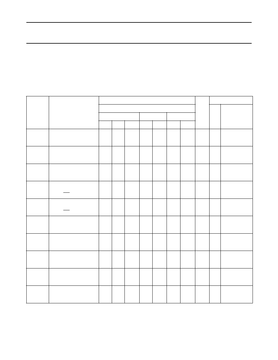
FUNCTION TABLE
Notes
1. H = HIGH voltage level
L = LOW voltage level
X = don't care
= LOW-to-HIGH transition
2. The data output functions may be enabled or disabled by various signals at OE
AB
and OE
BA
inputs. Data input
functions are always enabled, i.e., data at the bus inputs will be stored on every LOW-to-HIGH transition on the clock
inputs.
INPUTS
(1)
DATA I/O
(2)
OPERATION OR FUNCTION
OE
AB
OE
BA
CP
AB
CP
BA
S
AB
S
BA
A
1
THRU A
8
B
1
THRU B
8
HC/HCT652
L
H
H or L
H or L
X
X
Input
Input
Isolation
L
H
X
X
Store A and B data
X
H
H or L
X
X
Input
Not specified
Store A, Hold B
H
H
L
X
Input
Output
Store A in both registers
L
X
H or L
X
X
Not specified
Input
Hold A, Store B
L
L
X
L
Ouput
Input
Store B in both registers
L
L
X
X
X
L
Ouput
Input
Real Time B Data to A Bus
L
L
X
H or L
X
H
Stored B Data to A Bus
H
H
X
X
L
X
Input
Output
Real Time A Data to B Bus
H
H
H or L
X
H
X
Stored A Data to B Bus
H
L
H or L
H or L
H
H
Output
Output
Stored A Data to B Bus and
Stored B Data to A Bus
Fig.4 Functional diagram.
September 1993
5
Philips Semiconductors
Product specification
Octal bus transceiver/register; 3-state
74HC/HCT652
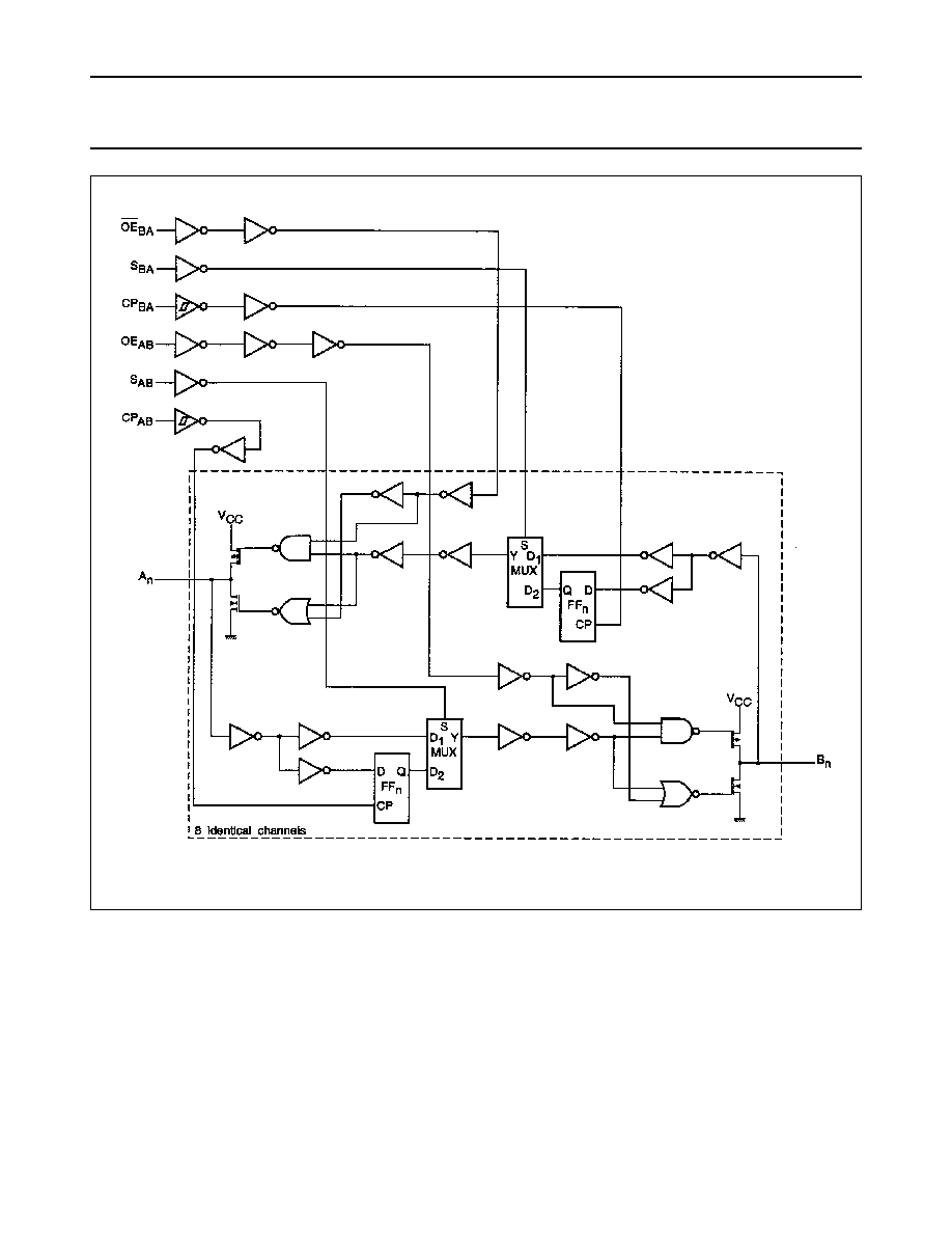
Fig.5 Logic diagram.
September 1993
6
Philips Semiconductors
Product specification
Octal bus transceiver/register; 3-state
74HC/HCT652
DC CHARACTERISTICS FOR 74HC
For the DC characteristics see
"74HC/HCT/HCU/HCMOS Logic Family Specifications"
.
Output capability: bus driver
I
CC
category: MSI.
AC CHARACTERISTICS FOR 74HC
GND = 0 V; t
r
= t
f
= 6 ns; C
L
= 50 pF.
SYMBOL
PARAMETER
T
amb
(
∞
C)
UNIT
TEST CONDITIONS
74HC
V
CC
(V)
WAVEFORMS
+
25
-
40 to
+
85
-
40 to
+
125
MIN. TYP.
MAX.
MIN. MAX.
MIN.
MAX.
t
PHL
/t
PLH
propagation delay
A
n
, B
n
to B
n
, A
n
-
-
-
44
16
13
135
27
23
-
-
-
170
34
29
-
-
-
205
41
35
ns
2.0
4.5
6.0
Fig.6
t
PHL
/t
PLH
propagation delay
CP
AB
, CP
BA
to B
n
, A
n
-
-
-
61
22
18
190
38
32
-
-
-
240
48
41
-
-
-
285
57
48
ns
2.0
4.5
6.0
Fig.7
t
PHL
/t
PLH
propagation delay
S
AB
, S
BA
to B
n
, A
n
-
-
-
63
23
18
195
39
33
-
-
-
245
49
42
-
-
-
295
59
50
ns
2.0
4.5
6.0
Fig.8
t
PZH
/t
PZL
3-state output enable
time
OE
AB
, OE
BA
to A
n
, B
n
-
-
-
47
17
14
150
30
26
-
-
-
190
38
33
-
-
-
225
45
38
ns
2.0
4.5
6.0
Fig.9
t
PHZ
/t
PLZ
3-state output disable
time
OE
AB
, OE
BA
to A
n
, B
n
-
-
-
41
15
12
150
30
26
-
-
-
190
38
33
-
-
-
225
45
38
ns
2.0
4.5
6.0
Fig.9
t
THL
/t
TLH
output transition time
-
-
-
14
5
4
60
12
10
-
-
-
75
15
13
-
-
-
90
18
15
ns
2.0
4.5
6.0
Figs 6, 8
t
W
clock pulse width
HIGH or LOW
CP
AB
or CP
BA
80
16
14
17
6
5
-
-
-
100
20
17
-
-
-
120
24
20
-
-
-
ns
2.0
4.5
6.0
Fig.7
t
su
set-up time
A
n
, B
n
to CP
AB
, CP
BA
100
20
17
17
6
5
-
-
-
125
25
21
-
-
-
150
30
26
-
-
-
ns
2.0
4.5
6.0
Fig.7
t
h
hold time
A
n
, B
n
to CP
AB
, CP
BA
25
5
4
-
8
-
3
-
2
-
-
-
30
6
5
-
-
-
35
7
6
-
-
-
ns
2.0
4.5
6.0
Fig.7
f
max
maximum clock pulse
frequency
6.0
30
35
16
83
98
-
-
-
4.8
24
28
-
-
-
4.0
20
24
-
-
-
MHz
2.0
4.5
6.0
Fig.7
September 1993
7
Philips Semiconductors
Product specification
Octal bus transceiver/register; 3-state
74HC/HCT652
DC CHARACTERISTICS FOR 74HCT
For the DC characteristics see
"74HC/HCT/HCU/HCMOS Logic Family Specifications"
.
Output capability: bus driver
I
CC
category: MSI.
Note to the HCT types
The value of additional quiescent supply current (
I
CC
) for unit a load of 1 is given in the family specifications.
To determine
I
CC
per input, multiply this value by the unit load coefficient shown in the table below
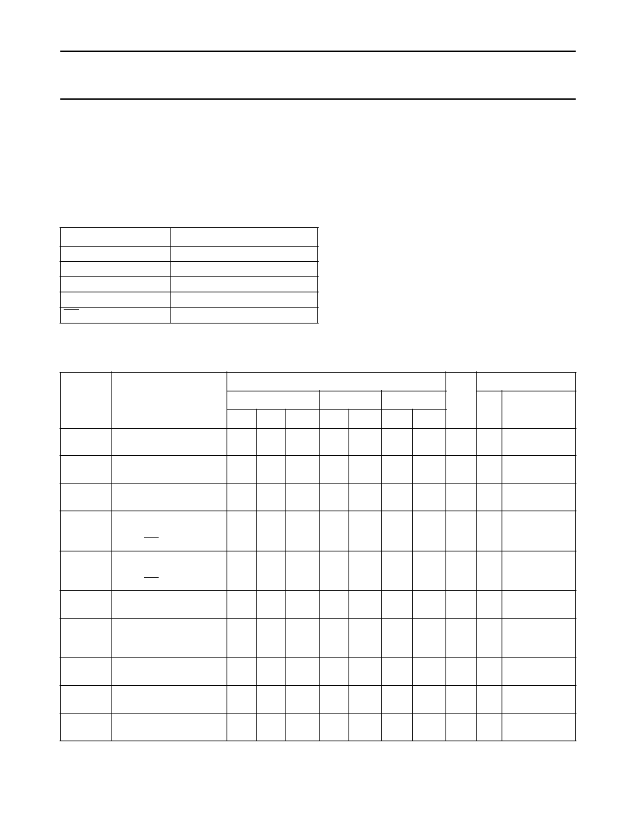
AC CHARACTERISTICS FOR 74HCT
GND = 0 V; t
r
= t
f
= 6 ns; C
L
= 50 pF.
INPUT
UNIT LOAD COEFFICIENT
S
AB
, S
BA
0.75
A
0
to A
7
and B
0
to B
7
0.75
CP
AB
, CP
BA
1.50
OE
AB
1.50
OE
BA
1.50
INPUT
PARAMETER
T
amb
(
∞
C)
UNIT
TEST CONDITIONS
+
25
-
40 to
+
85
-
40 to
+
125
V
CC
(V)
WAVEFORMS
MIN. TYP. MAX.
MIN. MAX. MIN.
MAX.
t
PHL
/t
PLH
propagation delay
A
n
, B
n
to B
n
, A
n
-
16
27
-
34
-
41
ns
4.5
Fig.6
t
PHL
/t
PLH
propagation delay
CP
AB
, CP
BA
to B
n
, A
n
-
23
39
-
49
-
59
ns
4.5
Fig.7
t
PHL
/t
PLH
propagation delay
S
AB
, S
BA
to B
n
, A
n
-
27
46
-
55
-
66
ns
4.5
Fig.8
t
PZH
/t
PZL
3-state output enable
time
OE
AB
, OE
BA
to A
n
, B
n
-
18
33
-
41
-
50
ns
4.5
Fig.9
t
PHZ
/t
PLZ
3-state output disable
time
OE
AB
, OE
BA
to A
n
, B
n
-
16
35
-
44
-
53
ns
4.5
Fig.9
t
THL
/t
TLH
output transition time
-
5
12
-
15
-
18
ns
4.5
Fig.6, 8
t
W
clock pulse width
HIGH or LOW
CP
AB
or CP
BA
16
6
-
20
-
24
-
ns
4.5
Fig.7
t
su
set-up time
A
n
, B
n
to CP
AB
, CP
BA
10
5
-
13
-
15
-
ns
4.5
Fig.7
t
h
hold time
A
n
, B
n
to CP
AB
, CP
BA
5
-
2
-
6
-
8
-
ns
4.5
Fig.7
f
max
maximum clock pulse
frequency
30
83
-
24
-
20
-
MHz
4.5
Fig.7

September 1993
8
Philips Semiconductors
Product specification
Octal bus transceiver/register; 3-state
74HC/HCT652
Fig.6
Waveforms showing the input A
n
, B
n
to
output B
n
, A
n
propagation delay times and
the output transition times.
(1) HC: V
M
= 50%; V
I
= GND to V
CC
.
HCT: V
M
= 1.3 V; V
I
= GND to 3 V.
Fig.7
Waveforms showing the A
n
, B
n
to CP
AB
,
CP
BA
set-up and hold times, clock CP
AB
,
CP
BA
pulse width, maximum clock pulse
frequency and the CP
AB
, CP
BA
to output B
n
,
A
n
propagation delays.
(1) HC: V
M
= 50%; V
I
= GND to V
CC
.
HCT: V
M
= 1.3 V; V
I
= GND to 3 V.
Fig.8
Waveforms showing the input S
AB
, S
BA
to
output B
n
, A
n
propagation delay times and
the output transition times.
(1) HC: V
M
= 50%; V
I
= GND to V
CC
.
HCT: V
M
= 1.3 V; V
I
= GND to 3 V.
Fig.9
Waveforms showing the output enable
inputs (OE
AB
, OE
BA
) to outputs A
n
, B
n
enable and disable times and the input
rise and fall times.
(1) HC: V
M
= 50%; V
I
= GND to V
CC
.
HCT: V
M
= 1.3 V; V
I
= GND to 3 V.

September 1993
9
Philips Semiconductors
Product specification
Octal bus transceiver/register; 3-state
74HC/HCT652
APPLICATION INFORMATION
Fig.10 Application information.

September 1993
10
Philips Semiconductors
Product specification
Octal bus transceiver/register; 3-state
74HC/HCT652
PACKAGE OUTLINES
See
"74HC/HCT/HCU/HCMOS Logic Package Outlines"
.