DATA SHEET
Product specification
File under Integrated Circuits, IC06
December 1990
INTEGRATED CIRCUITS
74HC/HCT670
4 x 4 register file; 3-state
For a complete data sheet, please also download:
∑
The IC06 74HC/HCT/HCU/HCMOS Logic Family Specifications
∑
The IC06 74HC/HCT/HCU/HCMOS Logic Package Information
∑
The IC06 74HC/HCT/HCU/HCMOS Logic Package Outlines
December 1990
2
Philips Semiconductors
Product specification
4 x 4 register file; 3-state
74HC/HCT670
FEATURES
∑
Simultaneous and independent read and write
operations
∑
Expandable to almost any word size and bit length
∑
Output capability: bus driver
∑
I
CC
category: MSI
GENERAL DESCRIPTION
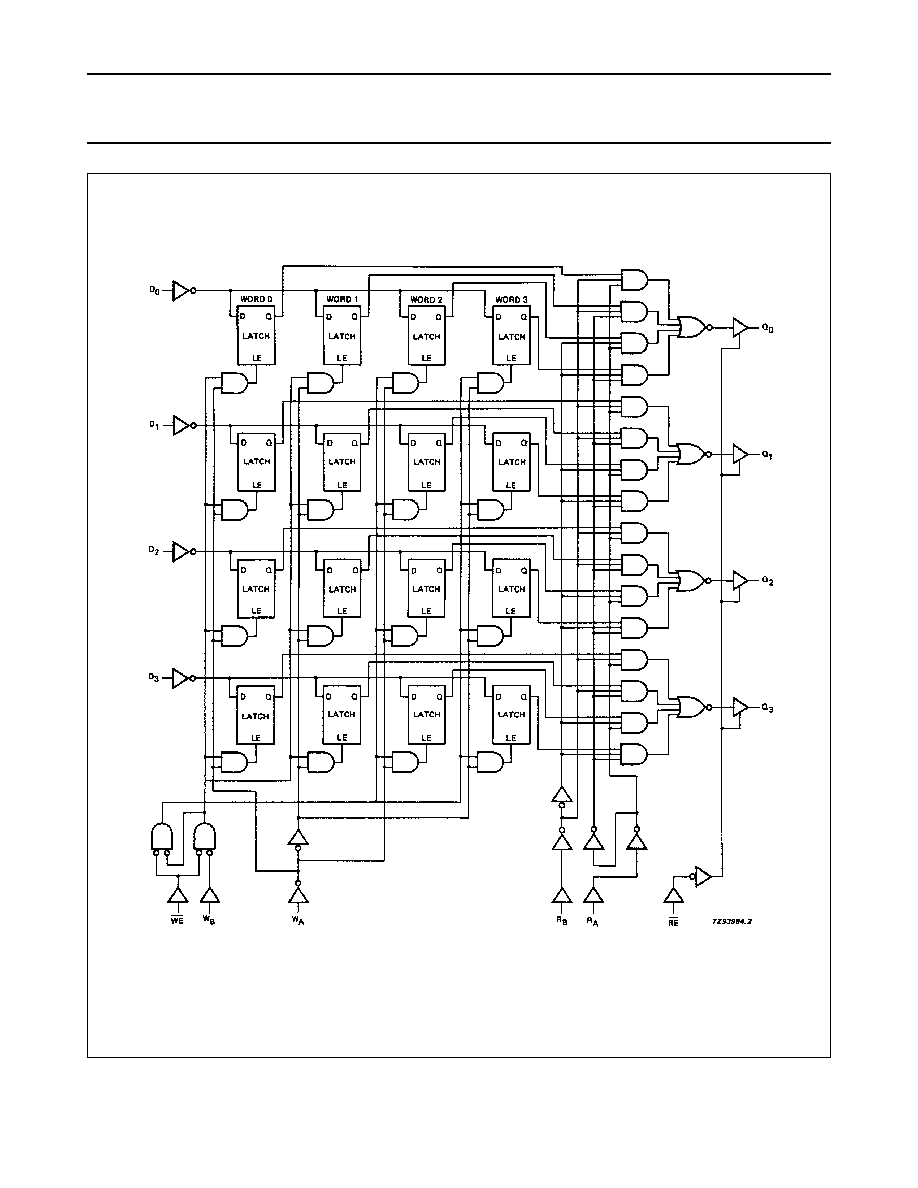
The 74HC/HCT670 are high-speed Si-gate CMOS devices
and are pin compatible with low power Schottky TTL
(LSTTL). They are specified in compliance with JEDEC
standard no. 7A.
The 74HC/HCT670 are 16-bit 3-state register files
organized as 4 words of 4 bits each. Separated read and
write address inputs (R
A
, R
B
and W
A
, W
B
) and enable
inputs (RE and WE) are available, permitting simultaneous
writing into one word location and reading from another
location. The 4-bit word to be stored is presented to four
data inputs (D
0
to D
3
). The W
A
and W
B
inputs determine
the location of the stored word. When the WE input is
LOW, the data is entered into the addressed location. The
addressed location remains transparent to the data while
the WE input is LOW. Data supplied at the inputs will be
read out in true (non-inverting) form from the 3-state
outputs (Q
0
to Q
3
). D
n
and W
n
inputs are inhibited when
WE is HIGH.
Direct acquisition of data stored in any of the four registers
is made possible by individual read address inputs
(R
A
and R
B
). The addressed word appears at the four
outputs when the RE is LOW. Data outputs are in the high
impedance OFF-state when RE is HIGH. This permits
outputs to be tied together to increase the word capacity to
very large numbers.
Design of the read enable signals for the stacked devices
must ensure that there is no overlap in the LOW levels
which would cause more than one output to be active at
the same time. Parallel expansion to generate n-bit words
is accomplished by driving the enable and address inputs
of each device in parallel.
QUICK REFERENCE DATA
GND = 0 V; T
amb
= 25
∞
C; t
r
= t
f
= 6 ns
Notes
1. C
PD
is used to determine the dynamic power dissipation (P
D
in
µ
W):
P
D
= C
PD
◊
V
CC
2
◊
f
i
+
(C
L
◊
V
CC
2
◊
f
o
)
where:
f
i
= input frequency in MHz
f
o
= output frequency in MHz
(C
L
◊
V
CC
2
◊
f
o
) = sum of outputs
C
L
= output load capacitance in pF
V
CC
= supply voltage in V
2. For HC the condition is V
I
= GND to V
CC
;
for HCT the condition is V
I
= GND to V
CC
-
1.5 V
ORDERING INFORMATION
See
"74HC/HCT/HCU/HCMOS Logic Package Information"
.
SYMBOL
PARAMETER
CONDITIONS
TYPICAL
UNIT
HC
HCT
t
PHL
/ t
PLH
propagation delay D
n
to Q
n
C
L
= 15 pF; V
CC
= 5 V
23
23
ns
C
I
input capacitance
3.5
3.5
pF
C
PD
power dissipation capacitance per package
notes 1 and 2
122
124
pF
December 1990
3
Philips Semiconductors
Product specification
4 x 4 register file; 3-state
74HC/HCT670
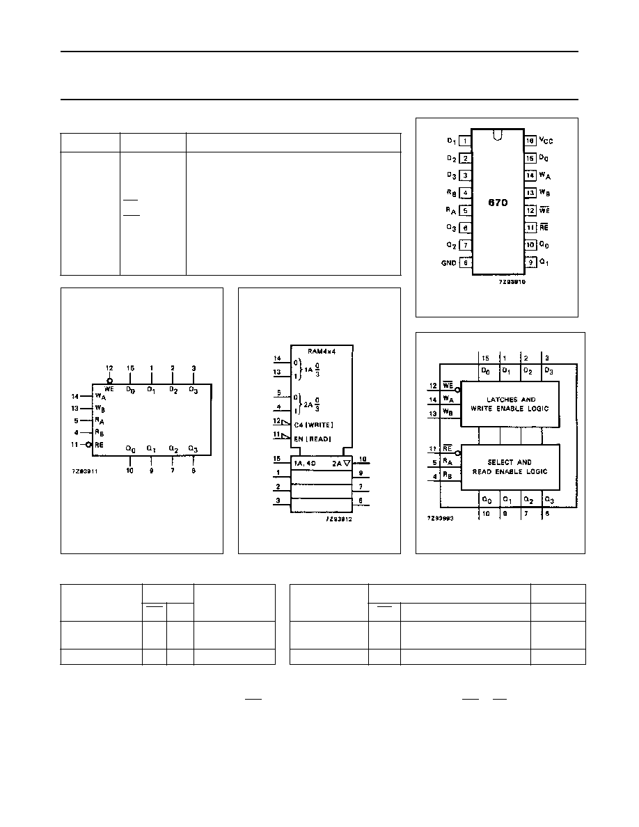
PIN DESCRIPTION
PIN NO.
SYMBOL
NAME AND FUNCTION
5, 4
R
A
, R
B
read address inputs
8
GND
ground (0 V)
10, 9, 7, 6
Q
0
to Q
3
data outputs
11
RE
3-state output read enable input (active LOW)
12
WE
write enable input (active LOW)
14, 13
W
A
, W
B
write address inputs
15, 1, 2, 3
D
0
to D
3
data inputs
16
V
CC
positive supply voltage
Fig.1 Pin configuration.
Fig.2 Logic symbol.
Fig.3 IEC logic symbol.
Fig.4 Functional diagram.
WRITE MODE SELECT TABLE
Note
1. The write address (W
A
and W
B
) to the
"internal latches" must be stable while WE is
LOW for conventional operation.
OPERATING
MODE
INPUTS
INTERNAL
LATCHES
(1)
WE
D
n
write data
L
L
L
H
L
H
data latched
H
X
no change
READ MODE SELECT TABLE
Notes
1. The selection of the "internal latches" by read address
(R
A
and R
B
) are not constrained by WE or RE operation.
H = HIGH voltage level
L = LOW voltage level
X = don't care
Z = high impedance OFF-state
OPERATING
MODE
INPUTS
OUTPUT
RE
INTERNAL LATCHES
(1)
Q
n
read
L
L
L
H
L
H
disabled
H
X
Z
December 1990
5
Philips Semiconductors
Product specification
4 x 4 register file; 3-state
74HC/HCT670
DC CHARACTERISTICS FOR 74HC
For the DC characteristics see
"74HC/HCT/HCU/HCMOS Logic Family Specifications"
.
Output capability: bus driver
I
CC
category: MSI
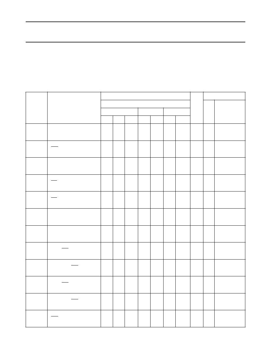
AC CHARACTERISTICS FOR 74HC
GND = 0 V; t
r
= t
f
= 6 ns; C
L
= 50 pF
SYMBOL
PARAMETER
T
amb
(
∞
C)
UNIT
TEST CONDITIONS
74HC
V
CC
(V)
WAVEFORMS
+
25
-
40 to
+
85
-
40 to
+
125
min.
typ.
max. min. max. min.
max.
t
PHL
/ t
PLH
propagation delay
R
A
, R
B
to Q
n
58
21
17
195
39
33
245
49
42
295
59
50
ns
2.0
4.5
6.0
Fig.6
t
PHL
/ t
PLH
propagation delay
WE to Q
n
77
28
22
250
50
43
315
63
54
375
75
64
ns
2.0
4.5
6.0
Fig.7
t
PHL
/ t
PLH
propagation delay
D
n
to Q
n
74
27
22
250
50
43
315
63
54
375
75
64
ns
2.0
4.5
6.0
Fig.7
t
PZH
/ t
PZL
3-state output enable time
RE to Q
n
39
14
11
150
30
26
190
38
33
225
45
38
ns
2.0
4.5
6.0
Fig.9
t
PHZ
/ t
PLZ
3-state output disable time
RE to Q
n
47
17
14
150
30
26
190
38
33
225
45
38
ns
2.0
4.5
6.0
Fig.9
t
THL
/ t
TLH
output transition time
14
5
4
60
12
10
75
15
13
90
18
15
ns
2.0
4.5
6.0
Fig.6
t
W
write enable pulse width
LOW
80
16
14
14
5
4
100
20
17
120
24
20
ns
2.0
4.5
6.0
Fig.8
t
su
set-up time
D
n
to WE
60
12
10
3
1
1
75
15
13
90
18
15
ns
2.0
4.5
6.0
Fig.8
t
su
set-up time
W
A
, W
B
to WE
60
12
10
6
2
2
75
15
13
90
18
15
ns
2.0
4.5
6.0
Fig.8
t
h
hold time
D
n
to WE
5
5
5
0
0
0
5
5
5
5
5
5
ns
2.0
4.5
6.0
Fig.8
t
h
hold time
W
A
, W
B
to WE
5
5
5
0
0
0
5
5
5
5
5
5
ns
2.0
4.5
6.0
Fig.8
t
latch
latch time
WE to R
A
, R
B
100
20
17
28
10
8
125
25
21
150
30
26
ns
2.0
4.5
6.0
Fig.8