 | –≠–ª–µ–∫—Ç—Ä–æ–Ω–Ω—ã–π –∫–æ–º–ø–æ–Ω–µ–Ω—Ç: 74HC7404 | –°–∫–∞—á–∞—Ç—å:  PDF PDF  ZIP ZIP |
Document Outline
- FEATURES
- APPLICATIONS
- GENERAL DESCRIPTION
- QUICK REFERENCE DATA
- ORDERING INFORMATION
- PINNING (SOT102)
- PINNING (SOT163A)
- FUNCTIONAL DESCRIPTION
- Expanded Format
- Parallel Expansion
- Serial Expansion
- DC CHARACTERISTICS FOR 74HC
- AC CHARACTERISTICS FOR 74HC
- DC CHARACTERISTICS FOR 74HCT
- UNIT LOAD COEFFICIENT
- AC CHARACTERISTICS FOR 74HCT
- AC WAVEFORMS
- Shifting in sequence FIFO empty to FIFO full
- With FIFO full; SI held HIGH in anticipation of empty location
- Master reset applied with FIFO full
- With FIFO empty; SO is held HIGH in anticipation
- Shift-in operation; high-speed burst mode
- Shift-out operation; high-speed burst mode
- APPLICATION INFORMATION
- Expanded format
- Sequence 1 (both FIFOS empty, starting SHIFT-IN process)
- Sequence 2 (FIFOB runs full)
- Sequence 3 (FIFOA runs full)
- Sequence 4 (both FIFOs full, starting SHIFT-OUT process)
- Sequence 5 (FIFOA runs empty)
- Sequence 6 (FIFOB runs empty)
- PACKAGE OUTLINES
DATA SHEET
Product specification
Supersedes data of October 1990
File under Integrated Circuits, IC06
September 1993
INTEGRATED CIRCUITS
74HC/HCT7404
5-Bit x 64-word FIFO register;
3-state
For a complete data sheet, please also download:
∑
The IC06 74HC/HCT/HCU/HCMOS Logic Family Specifications
∑
The IC06 74HC/HCT/HCU/HCMOS Logic Package Information
∑
The IC06 74HC/HCT/HCU/HCMOS Logic Package Outlines
September 1993
2
Philips Semiconductors
Product specification
5-Bit x 64-word FIFO register; 3-state
74HC/HCT7404
FEATURES
∑
Synchronous or asynchronous operation
∑
3-state outputs
∑
30 MHz (typical) shift-in and shift-out rates
∑
Readily expandable in word and bit dimensions
∑
Pinning arranged for easy board layout: input pins
directly opposite output pins
∑
Output capability: driver (8 mA)
∑
I
CC
category: LSI.
APPLICATIONS
∑
High-speed disc or tape controller
∑
Communications buffer.
GENERAL DESCRIPTION
The 74HC/HCT7404 are high-speed Si-gate CMOS
devices specified in compliance with JEDEC standard
no.7A.
The "7404" is an expandable, First-In First-Out (FIFO)
memory organized as 64 words by 5 bits. A guaranteed
15 MHz data-rate makes it ideal for high-speed
applications. A higher data-rate can be obtained in
applications where the status flags are not used
(burst-mode).
With separate controls for shift-in (SI) and shift-out (SO),
reading and writing operations are completely
independent, allowing synchronous and asynchronous
data transfers. Additional controls include a master-reset
input (MR), an output enable input (OE) and flags. The
data-in-ready (DIR) and data-out-ready (DOR) flags
indicate the status of the device.
QUICK REFERENCE DATA
GND = 0 V; T
amb
= 25
∞
C; t
r
= t
f
= 6 ns.
Note
1. For HC the condition is V
I
= GND to V
CC
.
For HCT the condition is V
I
= GND to V
CC
-
1.5 V.
ORDERING INFORMATION
SYMBOL
PARAMETER
CONDITIONS
TYP.
UNIT
HC
HCT
t
PHL
/t
PLH
propagation delay SO, SI to DIR and DOR
C
L
= 15 pF; V
CC
= 5 V
15
17
ns
f
max
maximum clock frequency
30
30
MHz
C
I
input capacitance
3.5
3.5
pF
C
PD
power dissipation capacitance per package
note 1
475
490
pF
EXTENDED
TYPE NUMBER
PACKAGE
PINS
PIN POSITION
MATERIAL
CODE
74HC/HCT7404N
18
DIL
plastic
SOT102
74HC/HCT7404D
20
SO20
plastic
SOT163A
September 1993
3
Philips Semiconductors
Product specification
5-Bit x 64-word FIFO register; 3-state
74HC/HCT7404
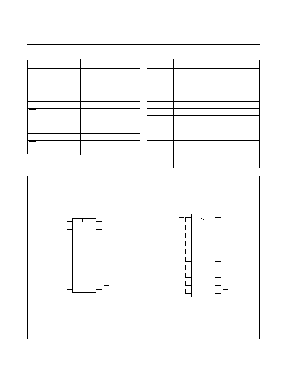
PINNING (SOT102)
SYMBOL
PIN
DESCRIPTION
OE
1
output enable input (active
LOW)
DIR
2
data-in-ready output
SI
3
shift-in input (active HIGH)
D
O
to D
4
4, 5, 6, 7, 8 parallel data inputs
GND
9
ground
MR
10
asynchronous master-reset
input (active LOW)
Q
4
to Q
0
11, 12, 13,
14, 15
data outputs
DOR
16
data-out-ready output
SO
17
shift-out input (active LOW)
V
CC
18
positive supply voltage
PINNING (SOT163A)
SYMBOL
PIN
DESCRIPTION
OE
1
output enable input (active
LOW)
DIR
2
data-in-ready output
SI
3
shift-in input (active HIGH)
n.c.
4
not connected
D
0
to D
4
5, 6, 7, 8, 9 parallel data inputs
GND
10
ground
MR
11
asynchronous master-reset
input (active LOW)
Q
4
to Q
0
12, 13, 14,
15, 16
data outputs
n.c.
17
not connected
DOR
18
data-out ready output
n.c.
19
not connected
V
CC
20
positive supply voltage
Fig.1 Pin configuration (SOT102).
handbook, halfpage
DIR
GND
VCC
D0
D 1
D 2
D 3
D 4
Q4
Q3
Q2
Q1
Q0
OE
7404
MGA670
SI
DOR
SO
MR
1
2
3
4
5
6
7
8
9
18
17
16
15
14
13
12
11
10
Fig.2 Pin configuration (SOT163).
handbook, halfpage
1
2
3
4
5
6
7
8
9
10
20
19
18
17
16
15
14
13
12
11
DIR
GND
V
CC
D0
D 1
D 2
D 3
D 4
Q4
Q3
Q2
Q1
Q0
OE
7404
MGA671
SI
n.c.
DOR
SO
n.c.
MR

September 1993
4
Philips Semiconductors
Product specification
5-Bit x 64-word FIFO register; 3-state
74HC/HCT7404
Fig.3 Logic symbol.
Pin numbers between parentheses refer to the SO package.
handbook, halfpage
MGA673
16 (18)
2 (2)
15 (16)
14 (15)
13 (14)
12 (13)
11 (12)
1 (1)
(3) 3
10 (11)
(19) 17
(5) 4
(6) 5
(7) 6
(8) 7
(9) 8
DIR
D0
D1
D2
D3
D4
Q4
Q3
Q2
Q1
Q0
OE
SI
DOR
SO
MR
Fig.4 IEC logic symbol.
Pin numbers between parentheses refer to the SO package.
handbook, halfpage
MGA675
1 ( /C2)
CT = 0
5
<
CT
64
>
CT 0
CTR
5Z6
1Z3
EN4
G1
G5
[IR] 3
[OR] 6
FIFO 64 x 5
2D
4
16 (18)
2 (2)
15 (16)
14 (15)
13 (14)
12 (13)
11 (12)
(1) 1
(3) 3
(11) 10
(19) 17
(5) 4
(6) 5
(7) 6
(8) 7
(9) 8
Fig.5 Functional diagram.
Pin numbers between parentheses refer to the SO package.
handbook, full pagewidth
MGA680
16 (18)
2 (2)
1 (1)
3 (3)
(11) 10
17 (19)
DIR
OE
SI
DOR
SO
MR
(5) 4
(6) 5
(7) 6
(8) 7
(9) 8
D0
D1
D2
D3
D4
15 (16)
14 (15)
13 (14)
12 (13)
11 (12)
Q4
Q3
Q2
Q1
Q0
INPUT
STAGE
1 x 5 BITS
MAIN FIFO
REGISTER
62 x 5 BITS
CONTROL LOGIC
OUTPUT
STAGE
1 x 5 BITS
OE

September 1993
5
Philips Semiconductors
Product specification
5-Bit x 64-word FIFO register; 3-state
74HC/HCT7404
full pagewidth
MSB117
(1)
R
SQ
FS
5
LATCHES
CL
CL
D
0
D
1
D
3
D
4
DIR
SI
MR
(2)
R
SQ
FF1
(2)
R
SQ
FF2
RQ
RQ
R
SQ
FF3
to
FF63
RQ
61 x
R
SQ
FF64
RQ
(2)
R
SQ
FB
(1)
R
SQ
FP
(1)
R
DOR
SO
OE
position 1
5
LATCHES
CL
CL
position 2
5
LATCHES
CL
CL
position 3 to 63
5
LATCHES
CL
CL
position 64
3-STATE
OUTPUT
BUFFER
Q
0
Q
1
Q
3
Q
4
Fig.6 Logic diagram.
(See control flip-flops)
LOW on
S input of flip-flops FS, FB and FP will set Q output to HIGH independent of state on
R input.
LOW on
R input of FF1 to FF64 will set Q output to LOW independent of state on
S input.