
DATA SHEET
Product specification
File under Integrated Circuits, IC06
December 1990
INTEGRATED CIRCUITS
74HC/HCT93
4-bit binary ripple counter
For a complete data sheet, please also download:
∑
The IC06 74HC/HCT/HCU/HCMOS Logic Family Specifications
∑
The IC06 74HC/HCT/HCU/HCMOS Logic Package Information
∑
The IC06 74HC/HCT/HCU/HCMOS Logic Package Outlines
December 1990
2
Philips Semiconductors
Product specification
4-bit binary ripple counter
74HC/HCT93
FEATURES
∑
Various counting modes
∑
Asynchronous master reset
∑
Output capability: standard
∑
I
CC
category: MSI
GENERAL DESCRIPTION
The 74HC/HCT93 are high-speed
Si-gate CMOS devices and are pin
compatible with low power Schottky
TTL (LSTTL). They are specified in
compliance with JEDEC standard
no. 7A.
The 74HC/HCT93 are 4-bit binary
ripple counters. The devices consist
of four master-slave flip-flops
internally connected to provide a
divide-by-two section and a
divide-by-eight section. Each section
has a separate clock input (CP
0
and
CP
1
) to initiate state changes of the
counter on the HIGH-to-LOW clock
transition. State changes of the Q
n
outputs do not occur simultaneously
because of internal ripple delays.
Therefore, decoded output signals
are subject to decoding spikes and
should not be used for clocks or
strobes.
A gated AND asynchronous master
reset (MR
1
and MR
2
) is provided
which overrides both clocks and
resets (clears) all flip-flops.
Since the output from the
divide-by-two section is not internally
connected to the succeeding stages,
the device may be operated in various
counting modes. In a 4-bit ripple
counter the output Q
0
must be
connected externally to input CP
1
.
The input count pulses are applied to
clock input CP
0
. Simultaneous
frequency divisions of 2, 4, 8 and 16
are performed at the Q
0
, Q
1
, Q
2
and
Q
3
outputs as shown in the function
table. As a 3-bit ripple counter the
input count pulses are applied to input
CP
1
.
Simultaneous frequency divisions of
2, 4 and 8 are available at the Q
1
, Q
2
and Q
3
outputs. Independent use of
the first flip-flop is available if the reset
function coincides with reset of the
3-bit ripple-through counter.
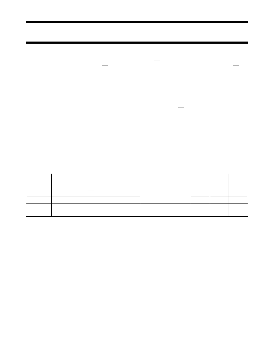
QUICK REFERENCE DATA
GND = 0 V; T
amb
= 25
∞
C; t
r
= t
f
= 6 ns
Notes
1. C
PD
is used to determine the dynamic power dissipation (P
D
in
µ
W):
P
D
= C
PD
◊
V
CC
2
◊
f
i
+
(C
L
◊
V
CC
2
◊
f
o
) where:
f
i
= input frequency in MHz; f
o
= output frequency in MHz
(C
L
◊
V
CC
2
◊
f
o
) = sum of outputs
C
L
= output load capacitance in pF; V
CC
= supply voltage in V
2. For HC the condition is V
I
= GND to V
CC
; for HCT the condition is V
I
= GND to V
CC
-
1.5 V
ORDERING INFORMATION
See
"74HC/HCT/HCU/HCMOS Logic Package Information"
.
SYMBOL
PARAMETER
CONDITIONS
TYPICAL
UNIT
HC
HCT
t
PHL
/ t
PLH
propagation delay CP
0
to Q
0
C
L
= 15 pF; V
CC
= 5 V
12
15
ns
f
max
maximum clock frequency
100
77
MHz
C
I
input capacitance
3.5
3.5
pF
C
PD
power dissipation capacitance per package
notes 1 and 2
22
22
pF
December 1990
5
Philips Semiconductors
Product specification
4-bit binary ripple counter
74HC/HCT93
DC CHARACTERISTICS FOR 74HC
For the DC characteristics see
"74HC/HCT/HCU/HCMOS Logic Family Specifications"
.
Output capability: standard
I
CC
category: MSI
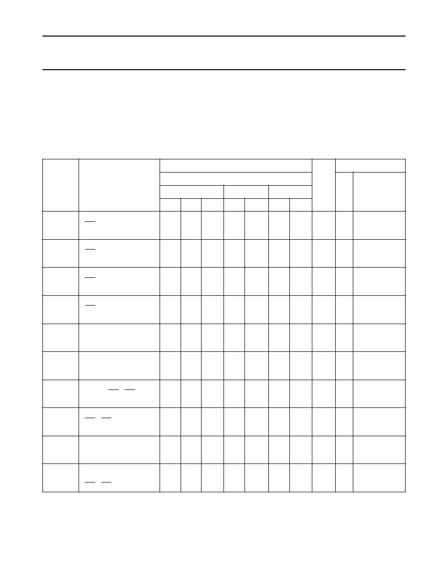
AC CHARACTERISTICS FOR 74HC
GND = 0 V; t
r
= t
f
= 6 ns; C
L
= 50 pF
SYMBOL
PARAMETER
T
amb
(
∞
C)
UNIT
TEST CONDITIONS
74HC
V
CC
(V)
WAVEFORMS
+
25
-
40 to
+
85
-
40 to
+
125
min.
typ.
max.
min.
max.
min.
max.
t
PHL
/ t
PLH
propagation delay
CP
0
to Q
0
41
15
12
125
25
21
155
31
26
190
38
32
ns
2.0
4.5
6.0
Fig.6
t
PHL
/ t
PLH
propagation delay
CP
1
to Q
1
49
16
13
135
27
23
170
34
29
205
41
35
ns
2.0
4.5
6.0
Fig.6
t
PHL
/ t
PLH
propagation delay
CP
1
to Q
2
61
22
18
185
37
31
230
46
39
280
56
48
ns
2.0
4.5
6.0
Fig.6
t
PHL
/ t
PLH
propagation delay
CP
1
to Q
3
80
29
23
245
49
42
305
61
52
370
71
63
ns
2.0
4.5
6.0
Fig.6
t
PHL
propagation delay
MR
n
to Q
n
50
18
14
155
31
26
195
39
33
235
47
40
ns
2.0
4.5
6.0
Fig.7
t
THL
/ t
TLH
output transition time
19
7
6
75
15
13
95
19
16
110
22
19
ns
2.0
4.5
6.0
Fig.6
t
rem
removal time
MR
n
to CP
0
, CP
1
50
10
9
8
3
2
65
13
11
75
15
13
ns
2.0
4.5
6.0
Fig.7
t
W
pulse width
CP
0
, CP
1
80
16
14
14
5
4
100
20
17
120
24
20
ns
2.0
4.5
6.0
Fig.6
t
W
master reset pulse width
MR
n
80
16
14
14
5
4
100
20
17
120
24
20
ns
2.0
4.5
6.0
Fig.7
f
max
maximum clock pulse
frequency
CP
0
, CP
1
6.0
30
35
30
91
108
4.8
24
28
4.0
20
24
MHz
2.0
4.5
6.0
Fig.6

