Document Outline
- FEATURES
- APPLICATIONS
- DESCRIPTION
- MARKING
- QUICK REFERENCE DATA
- PINNING
- LIMITING VALUES
- THERMAL CHARACTERISTICS
- CHARACTERISTICS
- PACKAGE OUTLINE
- DATA SHEET STATUS
- DEFINITIONS
- DISCLAIMERS

DATA SHEET
Product specification
Supersedes data of 2002 Aug 09
2002 Nov 22
DISCRETE SEMICONDUCTORS
BC817DS
NPN general purpose double
transistor
book, halfpage
M3D302

2002 Nov 22
2
Philips Semiconductors
Product specification
NPN general purpose double transistor
BC817DS
FEATURES
∑
High current (500 mA)
∑
600 mW total power dissipation
∑
Replaces two SOT23 packaged transistors on same
PCB area.
APPLICATIONS
∑
General purpose switching and amplification
∑
Push-pull amplifiers
∑
Multi-phase stepper motor drivers.
DESCRIPTION
NPN transistor pair in a SOT457 (SC-74) plastic package.
MARKING
TYPE NUMBER
MARKING CODE
BC817DS
N3
PINNING
PIN
DESCRIPTION
1, 4
emitter
TR1; TR2
2, 5
base
TR1; TR2
6, 3
collector
TR1; TR2
handbook, halfpage
1
3
2
4
5
6
Top view
MAM340
1
3
2
TR1
TR2
6
4
5
Fig.1
Simplified outline (SOT457) and symbol.
QUICK REFERENCE DATA
SYMBOL
PARAMETER
MAX.
UNIT
V
CEO
collector-emitter voltage
45
V
I
C
collector current (DC)
500
mA
I
CM
peak collector current
1
A
LIMITING VALUES
In accordance with the Absolute Maximum Rating System (IEC 60134).
Note
1. Device mounted on a printed-circuit board; single sided copper; tinplated; mounting pad for collector 1 cm
2
.
SYMBOL
PARAMETER
CONDITIONS
MIN.
MAX.
UNIT
Per transistor unless otherwise specified
V
CBO
collector-base voltage
open emitter
-
50
V
V
CEO
collector-emitter voltage
open base
-
45
V
V
EBO
emitter-base voltage
open collector
-
5
V
I
C
collector current (DC)
-
500
mA
I
CM
peak collector current
-
1
A
I
BM
peak base current
-
200
mA
P
tot
total power dissipation
T
amb
25
∞
C; note 1
-
370
mW
T
stg
storage temperature
-
65
+150
∞
C
T
j
junction temperature
-
150
∞
C
T
amb
operating ambient temperature
-
65
+150
∞
C
Per device
P
tot
total power dissipation
T
amb
25
∞
C; note 1
-
600
mW

2002 Nov 22
3
Philips Semiconductors
Product specification
NPN general purpose double transistor
BC817DS
THERMAL CHARACTERISTICS
Note
1. Device mounted on a printed-circuit board; single sided copper; tinplated; mounting pad for collector 1 cm
2
.
CHARACTERISTICS
T
amb
= 25
∞
C unless otherwise specified.
Notes
1. Pulse test: t
p
300
µ
s;
0.02.
2. V
BE
decreases by approximately
-
2 mV/K with increasing temperature.
SYMBOL
PARAMETER
CONDITIONS
VALUE
UNIT
R
th j-a
thermal resistance from junction to
ambient
note 1
208
K/W
SYMBOL
PARAMETER
CONDITIONS
MIN.
TYP.
MAX.
UNIT
Per transistor
I
CBO
collector-base cut-off current
V
CB
= 20 V; I
E
= 0
-
-
100
nA
V
CB
= 20 V; I
E
= 0; T
j
= 150
∞
C
-
-
5
µ
A
I
EBO
emitter-base cut-off current
V
EB
= 5 V; I
C
= 0
-
-
100
nA
h
FE
DC current gain
V
CE
= 1 V; I
C
= 100 mA; note 1
160
-
400
V
CE
= 1 V; I
C
= 500 mA; note 1
40
-
-
V
CEsat
collector-emitter saturation voltage I
C
= 500 mA; I
B
= 50 mA; note 1
-
-
700
mV
V
BE
base-emitter voltage
V
CE
= 1 V; I
C
= 500 mA;
notes 1 and 2
-
-
1.2
V
C
c
collector capacitance
V
CB
= 10 V; I
E
= I
e
= 0; f = 1 MHz
-
5
-
pF
f
T
transition frequency
V
CE
= 5 V; I
C
= 10 mA;
f = 100 MHz
100
-
-
MHz

2002 Nov 22
4
Philips Semiconductors
Product specification
NPN general purpose double transistor
BC817DS
handbook, halfpage
0
500
100
200
300
400
MBL747
10
-
1
1
10
10
2
IC (mA)
hFE
10
3
(3)
(1)
(2)
Fig.2
DC current gain as a function of collector
current; typical values.
V
CE
= 1 V.
(1) T
amb
= 150
∞
C.
(2) T
amb
= 25
∞
C.
(3) T
amb
=
-
55
∞
C.
handbook, halfpage
0
10
1000
0
200
400
600
800
2
4
6
8
VCE (V)
IC
(mA)
MBL748
(1) (2) (3) (4) (5)
(6)
(7)
(8)
(9)
(10)
Fig.3
Collector current as a function of
collector-emitter voltage; typical values.
(1) I
B
= 15 mA.
(2) I
B
= 13.5 mA.
(3) I
B
= 12 mA.
(4) I
B
= 10.5 mA.
(5) I
B
= 9 mA.
(6) I
B
= 7.5 mA.
(7) I
B
= 6 mA.
(8) I
B
= 4.5 mA.
(9) I
B
= 3 mA.
(10) I
B
= 1.5 mA.
handbook, halfpage
10
3
10
2
10
MBL749
10
-
1
1
10
IC (mA)
VCEsat
(mV)
10
2
10
3
(1)
(2)
(3)
Fig.4
Collector-emitter saturation voltage as a
function of collector current; typical values.
I
C
/I
B
= 10.
(1) T
amb
= 150
∞
C.
(2) T
amb
= 25
∞
C.
(3) T
amb
=
-
55
∞
C.
handbook, halfpage
200
1200
400
600
800
1000
MBL750
10
-
1
1
10
IC (mA)
VBE
(mV)
10
2
10
3
(1)
(2)
(3)
Fig.5
Base-emitter voltage as a function of
collector current; typical values.
V
CE
= 1 V.
(1) T
amb
=
-
55
∞
C.
(2) T
amb
= 25
∞
C.
(3) T
amb
= 150
∞
C.
2002 Nov 22
5
Philips Semiconductors
Product specification
NPN general purpose double transistor
BC817DS
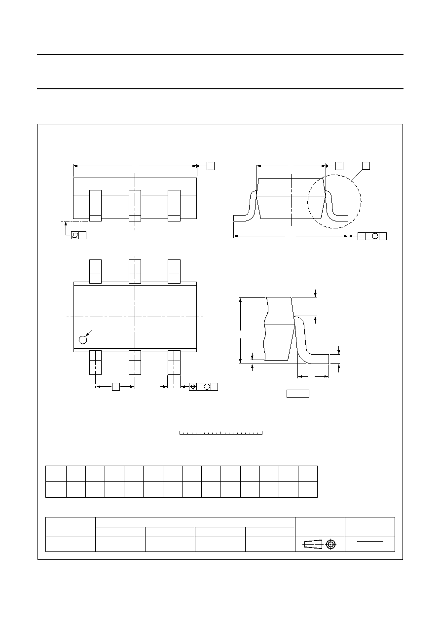
PACKAGE OUTLINE
REFERENCES
OUTLINE
VERSION
EUROPEAN
PROJECTION
ISSUE DATE
IEC
JEDEC
EIAJ
SOT457
SC-74
w
B
M
bp
D
e
pin 1
index
A
A1
Lp
Q
detail X
HE
E
v
M
A
A
B
y
0
1
2 mm
scale
c
X
1
3
2
4
5
6
Plastic surface mounted package; 6 leads
SOT457
UNIT
A1
bp
c
D
E
HE
Lp
Q
y
w
v
mm
0.1
0.013
0.40
0.25
3.1
2.7
0.26
0.10
1.7
1.3
e
0.95
3.0
2.5
0.2
0.1
0.2
DIMENSIONS (mm are the original dimensions)
0.6
0.2
0.33
0.23
A
1.1
0.9
97-02-28
01-05-04