December 1990
2
Philips Semiconductors
Product specification
9-bit x 64-word FIFO register; 3-state
74HC/HCT7030
FEATURES
∑
Synchronous or asynchronous operation
∑
3-state outputs
∑
Master-reset input to clear control functions
∑
33 MHz (typ.) shift-in, shift-out rates with or without flags
∑
Very low power consumption
∑
Cascadable to 25 MHz (typ.)
∑
Readily expandable in word and bit dimensions
∑
Pinning arranged for easy board layout: input pins
directly opposite output pins
∑
Output capability: standard
∑
I
CC
category: LSI
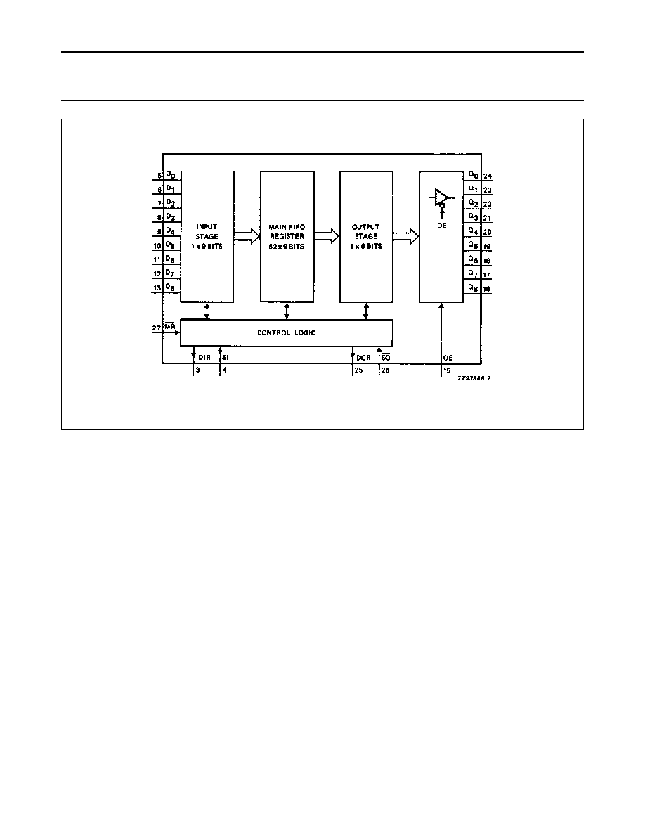
GENERAL DESCRIPTION
The 74HC/HCT7030 are high-speed Si-gate CMOS
devices specified in compliance with JEDEC standard
no. 7A.
The 74HC/HCT7030 is an expandable, First-In First-Out
(FIFO) memory organized as 64 words by 9 bits. A 33 MHz
data-rate makes it ideal for high-speed applications. Even
at high frequencies, the I
CC
dynamic is very low
(f
max
= 18 MHz; V
CC
= 5 V produces a dynamic I
CC
of
80 mA). If the device is not continuously operating at f
max
,
then I
CC
will decrease proportionally.
With separate controls for shift-in (SI) and shift-out (SO),
reading and writing operations are completely
independent, allowing synchronous and asynchronous
data transfers. Additional controls include a master-reset
input (MR) and an output enable input (OE). Flags for
data-in-ready (DIR) and data-out-ready (DOR) indicate the
status of the device.
Devices can be interconnected easily to expand word and
bit dimensions. All output pins are directly opposite the
corresponding input pins thus simplifying board layout in
expanded applications.
INPUTS AND OUTPUTS
Data inputs (D
0
to D
8
)
As there is no weighting of the inputs, any input can be
assigned as the MSB. The size of the FIFO memory can
be reduced from the 9
◊
64 configuration, i.e. 8
◊
64,
7
◊
64, down to 1
◊
64, by tying unused data input pins to
V
CC
or GND.
Data outputs (Q
0
to Q
8
)
As there is no weighting of the outputs, any output can be
assigned as the MSB. The size of the FIFO memory can
be reduced from the 9
◊
64 configuration as described for
data inputs. In a reduced format, the unused data output
pins must be left open circuit.
Master-reset (MR)
When MR is LOW, the control functions within the FIFO
are cleared, and data content is declared invalid. The
data-in-ready (DIR) flag is set HIGH and the
data-out-ready (DOR) flag is set LOW. The output stage
remains in the state of the last word that was shifted out,
or in the random state existing at power-up.
Status flag outputs (DIR, DOR)
Indication of the status of the FIFO is given by two status
flags, data-in-ready (DIR) and data-out-ready (DOR):
Shift-in control (SI)
Data is loaded into the input stage on a LOW-to-HIGH
transition of SI. A HIGH-to-LOW transition triggers an
automatic data transfer process (ripple through). If SI is
held HIGH during reset, data will be loaded at the rising
edge of the MR signal.
Shift-out control (SO)
A LOW-to-HIGH transition of SO causes the DOR flags to
go LOW. A HIGH-to-LOW transition of SO causes
upstream data to move into the output stage, and empty
locations to move towards the input stage (bubble-up).
Output enable (OE)
The outputs Q
0
to Q
8
are enabled when OE = LOW. When
OE = HIGH the outputs are in the high impedance
OFF-state.
DIR
= HIGH indicates the input stage is empty and
ready to accept valid data
DIR
= LOW indicates that the FIFO is full or that a
previous shift-in operation is not complete
(busy)
DOR = HIGH assures valid data is present at the
outputs Q
0
to Q
8
(does not indicate that new
data is awaiting transfer into the output stage)
DOR = LOW indicates the output stage is busy or
there is no valid data
December 1990
4
Philips Semiconductors
Product specification
9-bit x 64-word FIFO register; 3-state
74HC/HCT7030
PIN DESCRIPTION
Note
1. Pin 14 must be connected to GND. Pins 1 and 2 can be left floating or connected to GND, however it is not allowed
to let current flow in either direction between pins 1, 2 and 14.
PIN NO.
SYMBOL
NAME AND FUNCTION
1, 2, 14
GND
ground (0 V)
3
DIR
data-in-ready output
4
SI
shift-in input (LOW-to-HIGH, edge-triggered)
5, 6, 7, 8, 9, 10, 11, 12, 13
D
0
to D
8
parallel data inputs
15
OE
output enable input (active LOW)
24, 23, 22, 21, 20, 19, 18, 17, 16
Q
0
to Q
8
3-state parallel data outputs
25
DOR
data-out-ready output
26
SO
shift-out input (HIGH-to-LOW, edge-triggered)
27
MR
asynchronous master-reset input (active LOW)
28
V
CC
positive supply voltage
Fig.1 Pin configuration.
Fig.2 Logic symbol.
Fig.3 IEC logic symbol.