Document Outline
- FEATURES
- GENERAL DESCRIPTION
- QUICK REFERENCE DATA
- ORDERING INFORMATION
- PIN DESCRIPTION
- FUNCTION TABLE
- DC CHARACTERISTICS
- AC CHARACTERISTICS
- AC WAVEFORMS
- PACKAGE OUTLINES
- SOT27-1
- SOT108-1
- SOT337-1
- SOT402-1
- SOLDERING
- DEFINITIONS
DATA SHEET
Product specification
Supersedes data of September 1993
File under Integrated Circuits, IC06
1998 Feb 23
INTEGRATED CIRCUITS
74HC/HCT74
Dual D-type flip-flop with set and
reset; positive-edge trigger
For a complete data sheet, please also download:
∑
The IC06 74HC/HCT/HCU/HCMOS Logic Family Specifications
1998 Feb 23
2
Philips Semiconductors
Product specification
Dual D-type flip-flop with set and reset;
positive-edge trigger
74HC/HCT74
FEATURES
∑
Output capability: standard
∑
I
CC
category: flip-flops
GENERAL DESCRIPTION
The 74HC/HCT74 are high-speed Si-gate CMOS devices
and are pin compatible with low power Schottky TTL
(LSTTL). They are specified in compliance with JEDEC
standard no. 7A.
The 74HC/HCT74 are dual positive-edge triggered, D-type
flip-flops with individual data (D) inputs, clock (CP) inputs,
set (S
D
) and reset (R
D
) inputs; also complementary Q and
Q outputs.
The set and reset are asynchronous active LOW inputs
and operate independently of the clock input. Information
on the data input is transferred to the Q output on the
LOW-to-HIGH transition of the clock pulse. The D inputs
must be stable one set-up time prior to the LOW-to-HIGH
clock transition for predictable operation.
Schmitt-trigger action in the clock input makes the circuit
highly tolerant to slower clock rise and fall times.
QUICK REFERENCE DATA
GND = 0 V; T
amb
= 25
∞
C; t
r
= t
f
= 6 ns
Notes
1. C
PD
is used to determine the dynamic power dissipation (P
D
in
µ
W):
P
D
= C
PD
◊
V
CC
2
◊
f
i
+
(C
L
◊
V
CC
2
◊
f
o
) where:
f
i
= input frequency in MHz
f
o
= output frequency in MHz
(C
L
◊
V
CC
2
◊
f
o
) = sum of outputs
C
L
= output load capacitance in pF
V
CC
= supply voltage in V
2. For HC the condition is V
I
= GND to V
CC
For HCT the condition is V
I
= GND to V
CC
-
1.5 V
SYMBOL
PARAMETER
CONDITIONS
TYPICAL
UNIT
HC
HCT
t
PHL
/ t
PLH
propagation delay
C
L
= 15 pF; V
CC
= 5 V
nCP to nQ, nQ
14
15
ns
nS
D
to nQ, nQ
15
18
ns
nR
D
to nQ, nQ
16
18
ns
f
max
maximum clock frequency
76
59
MHz
C
I
input capacitance
3.5
3.5
pF
C
PD
power dissipation capacitance per flip-flop
notes 1 and 2
24
29
pF
1998 Feb 23
3
Philips Semiconductors
Product specification
Dual D-type flip-flop with set and reset;
positive-edge trigger
74HC/HCT74
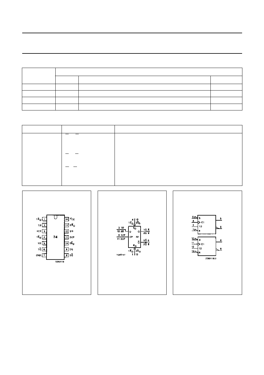
ORDERING INFORMATION
PIN DESCRIPTION
TYPE
NUMBER
PACKAGE
NAME
DESCRIPTION
VERSION
74HC(T)74N
DIP14
plastic dual in-line package; 14 leads (300 mil)
SOT27-1
74HC(T)74D
SO14
plastic small outline package; 14 leads; body width 3.9 mm
SOT108-1
74HCT74DB
SSOP14
plastic shrink small outline package; 14 leads; body width 5.3 mm
SOT337-1
74HCT74PW
TSSOP14
plastic thin shrink small outline package; 14 leads; body width 4.4 mm SOT402-1
PIN NO.
SYMBOL
NAME AND FUNCTION
1, 13
1R
D
, 2R
D
asynchronous reset-direct input (active LOW)
2, 12
1D, 2D
data inputs
3, 11
1CP, 2CP
clock input (LOW-to-HIGH, edge-triggered)
4, 10
1S
D
, 2S
D
asynchronous set-direct input (active LOW)
5, 9
1Q, 2Q
true flip-flop outputs
6, 8
1Q, 2Q
complement flip-flop outputs
7
GND
ground (0 V)
14
V
CC
positive supply voltage
Fig.1 Pin configuration.
Fig.2 Logic symbol.
Fig.3 IEC logic symbol.
1998 Feb 23
4
Philips Semiconductors
Product specification
Dual D-type flip-flop with set and reset;
positive-edge trigger
74HC/HCT74
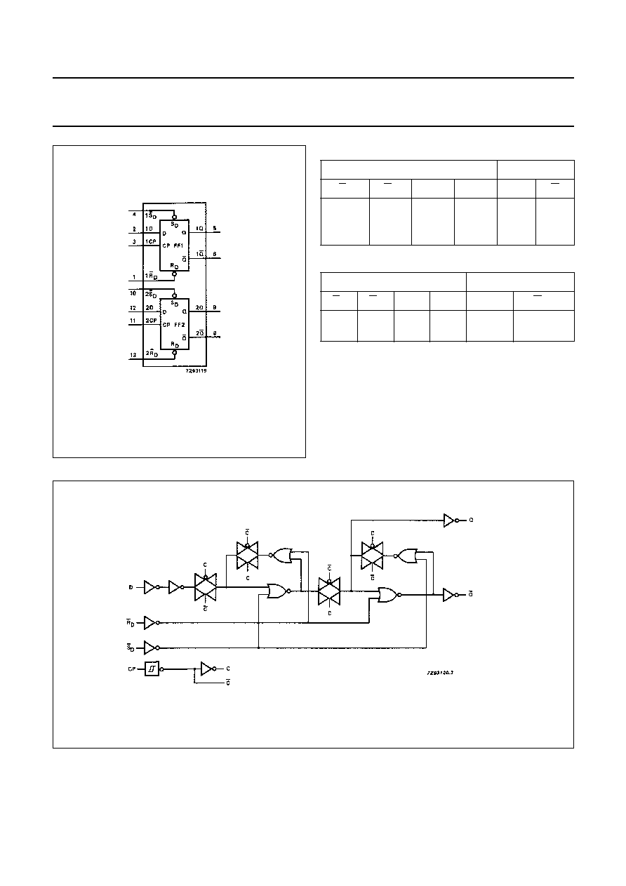
Fig.4 Functional diagram.
FUNCTION TABLE
Note
1. H = HIGH voltage level
L = LOW voltage level
X = don't care
= LOW-to-HIGH CP transition
Q
n
+
1
= state after the next LOW-to-HIGH CP transition
INPUTS
OUTPUTS
S
D
R
D
CP
D
Q
Q
L
H
X
X
H
L
H
L
X
X
L
H
L
L
X
X
H
H
INPUTS
OUTPUTS
S
D
R
D
CP
D
Q
n
+
1
Q
n
+
1
H
H
L
L
H
H
H
H
H
L
Fig.5 Logic diagram (one flip-flop).
1998 Feb 23
5
Philips Semiconductors
Product specification
Dual D-type flip-flop with set and reset;
positive-edge trigger
74HC/HCT74
DC CHARACTERISTICS FOR 74HC
For the DC characteristics see
"74HC/HCT/HCU/HCMOS Logic Family Specifications"
.
Output capability: standard
I
CC
category: flip-flops
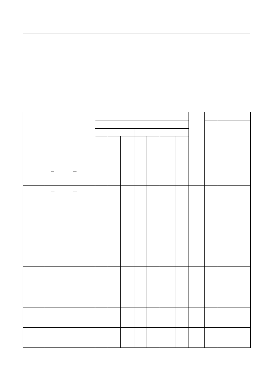
AC CHARACTERISTICS
GND = 0 V; t
r
= t
f
= 6 ns; C
L
= 50 pF
SYMBOL PARAMETER
T
amb
(
∞
C)
UNIT
TEST CONDITIONS
74HC
V
CC
(V)
WAVEFORMS
+
25
-
40 to
+
85
-
40 to
+
125
min.
typ.
max. min.
max
min.
max.
t
PHL
/ t
PLH
propagation delay
nCP to nQ, nQ
47
175
220
265
ns
2.0
Fig.6
17
35
44
53
4.5
14
30
37
45
6.0
t
PHL
/ t
PLH
propagation delay
nS
D
to nQ, nQ
50
200
250
300
ns
2.0
Fig.7
18
40
50
60
4.5
14
34
43
51
6.0
t
PHL
/ t
PLH
propagation delay
nR
D
to nQ, nQ
52
200
250
300
ns
2.0
Fig.7
19
40
50
60
4.5
15
34
43
51
6.0
t
THL
/ t
TLH
output transition time
19
75
95
110
ns
2.0
Fig.6
7
15
19
22
4.5
6
13
16
19
6.0
t
W
clock pulse width
HIGH or LOW
80
19
100
120
ns
2.0
Fig.6
16
7
20
24
4.5
14
6
17
20
6.0
t
W
set or reset pulse width
LOW
80
19
100
120
ns
2.0
Fig.7
16
7
20
24
4.5
14
6
17
20
6.0
t
rem
removal time
set or reset
30
3
40
45
ns
2.0
Fig.7
6
1
8
9
4.5
5
1
7
8
6.0
t
su
set-up time
nD to nCP
60
6
75
90
ns
2.0
Fig.6
12
2
15
18
4.5
10
2
13
15
6.0
t
h
hold time
nCP to nD
3
-
6
3
3
ns
2.0
Fig.6
3
-
2
3
3
4.5
3
-
2
3
3
6.0
f
max
maximum clock pulse
frequency
6.0
23
4.8
4.0
MHz
2.0
Fig.6
30
69
24
20
4.5
35
82
28
24
6.0