DATA SHEET
File under Integrated Circuits, IC06
March 1988
INTEGRATED CIRCUITS
FAMILY SPECIFICATIONS
HCMOS family characteristics
March 1988
2
Philips Semiconductors
HCMOS family characteristics
FAMILY
SPECIFICATIONS
GENERAL
These family specifications cover the common electrical
ratings and characteristics of the entire HCMOS
74HC/HCT/HCU family, unless otherwise specified in the
individual device data sheet.
INTRODUCTION
The 74HC/HCT/HCU high-speed Si-gate CMOS logic
family combines the low power advantages of the
HE4000B family with the high speed and drive capability of
the low power Schottky TTL (LSTTL).
The family will have the same pin-out as the 74 series and
provide the same circuit functions.
In these families are included several HE4000B family
circuits which do not have TTL counterparts, and some
special circuits.
The basic family of buffered devices, designated as
XX74HCXXXXX, will operate at CMOS input logic levels
for high noise immunity, negligible typical quiescent supply
and input current. It is operated from a power supply of
2 to 6 V.
A subset of the family, designated as XX74HCTXXXXX,
with the same features and functions as the "HC-types",
will operate at standard TTL power supply voltage
(5 V
�
10%) and logic input levels (0.8 to 2.0 V) for use as
pin-to-pin compatible CMOS replacements to reduce
power consumption without loss of speed. These types are
also suitable for converted switching from TTL to CMOS.
Another subset, the XX74HCUXXXXX, consists of
single-stage unbuffered CMOS compatible devices for
application in RC or crystal controlled oscillators and other
types of feedback circuits which operate in the linear
mode.
HANDLING MOS DEVICES
Inputs and outputs are protected against electrostatic
effects in a wide variety of device-handling situations.
However, to be totally safe, it is desirable to take handling
precautions into account
(see also
"HANDLING PRECAUTIONS").
RECOMMENDED OPERATING CONDITIONS FOR 74HC/HCT
Note
1. For analog switches, e.g. "4016", "4051 series", "4351 series", "4066" and "4067", the specified maximum operating
supply voltage is 10 V.
SYMBOL PARAMETER
74HC
74HCT
UNIT CONDITIONS
min. typ.
max.
min. typ.
max.
V
CC
DC supply voltage
2.0
5.0
6.0
4.5
5.0
5.5
V
V
I
DC input voltage range
0
V
CC
0
V
CC
V
V
O
DC output voltage range
0
V
CC
0
V
CC
V
T
amb
operating ambient temperature range
-
40
+
85
-
40
+
85
�
C
see DC and AC
CHAR. per device
T
amb
operating ambient temperature range
-
40
+
125
-
40
+
125
�
C
t
r
, t
f
input rise and fall times except for
Schmitt-trigger inputs
6.0
1000
6.0
500
ns
V
CC
= 2.0 V
500
V
CC
= 4.5 V
400
V
CC
= 6.0 V

March 1988
3
Philips Semiconductors
HCMOS family characteristics
FAMILY SPECIFICATIONS
RECOMMENDED OPERATING CONDITIONS FOR 74HCU
RATINGS
Limiting values in accordance with the Absolute Maximum System (IEC 134)
Voltages are referenced to GND (ground = 0 V)
Note
1. For analog switches, e.g. "4016", "4051 series", "4351 series", "4066" and "4067", the specified maximum operating
supply voltage is 11 V.
SYMBOL
PARAMETER
74HCU
UNIT CONDITIONS
min. typ. max.
V
CC
DC supply voltage
2.0
5.0
6.0
V
V
I
DC input voltage range
0
V
CC
V
V
O
DC output voltage range
0
V
CC
V
T
amb
operating ambient temperature range
-
40
+
85
�
C
see DC and AC
CHAR. per device
T
amb
operating ambient temperature range
-
40
+
125
�
C
SYMBOL
PARAMETER
MIN.
MAX.
UNIT CONDITIONS
V
CC
DC supply voltage
-
0.5
+
7
V
�
I
IK
DC input diode current
20
mA
for V
I
< -
0.5 or V
I
>
V
CC
+
0.5 V
�
I
OK
DC output diode current
20
mA
for V
O
< -
0.5 or V
O
>
V
CC
+
0.5 V
�
I
O
DC output source or sink
current
for
-
0.5 V
<
V
O
<
V
CC
+
0.5 V
standard outputs
25
mA
bus driver outputs
35
mA
�
I
CC
;
�
I
GND
DC V
CC
or GND current for
types with:
standard outputs
50
mA
bus driver outputs
70
mA
T
stg
storage temperature range
-
65
+
150
�
C
P
tot
power dissipation per package
for temperature range:
-
40 to
+
125
�
C
74HC/HCT/HCU
plastic DIL
750
mW
above
+
70
�
C: derate linearly with 12 mW/K
plastic mini-pack (SO)
500
mW
above
+
70
�
C: derate linearly with 8 mW/K

March 1988
4
Philips Semiconductors
HCMOS family characteristics
FAMILY SPECIFICATIONS
DC CHARACTERISTICS FOR 74HC
Voltages are referenced to GND (ground = 0 V)
SYMBOL PARAMETER
T
amb
(
�
C)
UNIT
TEST CONDITIONS
74HC
V
CC
(V)
V
I
OTHER
+
25
-
40 to
+
85
-
40 to
+
125
min. typ. max. min. max. min.
max.
V
IH
HIGH level input
voltage
1.5
1.2
1.5
1.5
V
2.0
3.15 2.4
3.15
3.15
4.5
4.2
3.2
4.2
4.2
6.0
V
IL
LOW level input
voltage
0.8
0.5
0.5
0.5
V
2.0
2.1
1.35
1.35
1.35
4.5
2.8
1.8
1.8
1.8
6.0
V
OH
HIGH level output
voltage
all outputs
1.9
2.0
1.9
1.9
V
2.0
V
IH
or
V
IL
-
I
O
= 20
�
A
4.4
4.5
4.4
4.4
4.5
-
I
O
= 20
�
A
5.9
6.0
5.9
5.9
6.0
-
I
O
= 20
�
A
V
OH
HIGH level output
voltage
standard outputs
3.98 4.32
3.84
3.7
V
4.5
V
IH
or
V
IL
-
I
O
= 4.0 mA
5.48 5.81
5.34
5.2
6.0
-
I
O
= 5.2 mA
V
OH
HIGH level output
voltage
bus driver outputs
3.98 4.32
3.84
3.7
V
4.5
V
IH
or
V
IL
-
I
O
= 6.0 mA
5.48 5.81
5.34
5.2
6.0
-
I
O
= 7.8 mA
V
OL
LOW level output
voltage
all outputs
0
0.1
0.1
0.1
V
2.0
V
IH
or
V
IL
I
O
= 20
�
A
0
0.1
0.1
0.1
4.5
I
O
= 20
�
A
0
0.1
0.1
0.1
6.0
I
O
= 20
�
A
V
OL
LOW level output
voltage
standard outputs
0.15 0.26
0.33
0.4
V
4.5
V
IH
or
V
IL
I
O
= 4.0 mA
0.16 0.26
0.33
0.4
6.0
I
O
= 5.2 mA
V
OL
LOW level output
voltage
bus driver outputs
0.15 0.26
0.33
0.4
V
4.5
V
IH
or
V
IL
I
O
= 6.0 mA
0.16 0.26
0.33
0.4
6.0
I
O
= 7.8 mA
�
I
I
input leakage current
0.1
1.0
1.0
�
A
6.0
V
CC
or
GND
�
I
OZ
3-state OFF-state
current
0.5
5.0
10.0
�
A
6.0
V
IH
or
V
IL
V
O
= V
CC
or GND
I
CC
quiescent supply
current
SSI
2.0
20.0
40.0
�
A
6.0
V
CC
or
GND
I
O
= 0
flip-flops
4.0
40.0
80.0
6.0
I
O
= 0
MSI
8.0
80.0
160.0
6.0
I
O
= 0
LSI
50.0
500
1000
6.0
I
O
= 0
March 1988
5
Philips Semiconductors
HCMOS family characteristics
FAMILY SPECIFICATIONS
DC CHARACTERISTICS FOR 74HCT
Voltages are referenced to GND (ground = 0 V)
SYMBOL PARAMETER
T
amb
(
�
C)
UNIT
TEST CONDITIONS
74HCT
V
CC
(V)
V
I
OTHER
+
25
-
40 to
+
85
-
40 to
+
125
min.
typ.
max. min. max. min.
max.
V
IH
HIGH level input
voltage
2.0
1.6
2.0
2.0
V
4.5
to
5.5
V
IL
LOW level input
voltage
1.2
0.8
0.8
0.8
V
4.5
to
5.5
V
OH
HIGH level output
voltage
all outputs
4.4
4.5
4.4
4.4
V
4.5
V
IH
or
V
IL
-
I
O
= 20
�
A
V
OH
HIGH level output
voltage
standard outputs
3.98
4.32
3.84
3.7
V
4.5
V
IH
or
V
IL
-
I
O
= 4.0 mA
V
OH
HIGH level output
voltage
bus driver outputs
3.98
4.32
3.84
3.7
V
4.5
V
IH
or
V
IL
-
I
O
= 6.0 mA
V
OL
LOW level output
voltage
all outputs
0
0.1
0.1
0.1
V
4.5
V
IH
or
V
IL
I
O
= 20
�
A
V
OL
LOW level output
voltage
standard outputs
0.15
0.26
0.33
0.4
V
4.5
V
IH
or
V
IL
I
O
= 4.0 mA
V
OL
LOW level output
voltage
bus driver outputs
0.16
0.26
0.33
0.4
V
4.5
V
IH
or
V
IL
I
O
= 6.0 mA
�
I
I
input leakage
current
0.1
1.0
1.0
�
A
5.5
V
CC
or
GND
�
I
OZ
3-state OFF-state
current
0.5
5.0
10.0
�
A
5.5
V
IH
or
V
IL
V
O
= V
CC
or
GND per input
pin;
other inputs at
V
CC
or GND;
I
O
= 0
I
CC
quiescent supply
current
SSI
2.0
20.0
40.0
�
A
5.5
V
CC
or
GND
I
O
= 0
flip-flops
4.0
40.0
80.0
5.5
I
O
= 0
MSI
8.0
80.0
160.0
5.5
I
O
= 0
LSI
50.0
500
1000
5.5
I
O
= 0
March 1988
6
Philips Semiconductors
HCMOS family characteristics
FAMILY SPECIFICATIONS
Note
1. The additional quiescent supply current per input is determined by the
I
CC
unit load, which has to be multiplied by
the unit load coefficient as given in the individual data sheets. For dual supply systems the theoretical worst-case
(V
I
= 2.4 V; V
CC
= 5.5 V) specification is:
I
CC
= 0.65 mA (typical) and 1.8 mA (maximum) across temperature.
I
CC
additional quiescent
supply current per
input pin for unit load
coefficient is 1
(note 1)
100
360
450
490
�
A
4.5
to
5.5
V
CC
-
2.1 V
other inputs at
V
CC
or GND;
I
O
= 0
SYMBOL PARAMETER
T
amb
(
�
C)
UNIT
TEST CONDITIONS
74HCT
V
CC
(V)
V
I
OTHER
+
25
-
40 to
+
85
-
40 to
+
125
min.
typ.
max. min. max. min.
max.

March 1988
7
Philips Semiconductors
HCMOS family characteristics
FAMILY SPECIFICATIONS
DC CHARACTERISTICS FOR 74HCU
Voltages are referenced to GND (ground = 0 V)
SYMBOL
PARAMETER
T
amb
(
�
C)
UNIT
TEST CONDITIONS
74HCU
V
CC
(V)
V
I
OTHER
+
25
-
40 to
+
85
-
40 to
+
125
min. typ. max. min. max. min.
max.
V
IH
HIGH level input
voltage
1.7
1.4
1.7
1.7
V
2.0
3.6
2.6
3.6
3.6
4.5
4.8
3.4
4.8
4.8
6.0
V
IL
LOW level input
voltage
0.6
0.3
0.3
0.3
V
2.0
1.9
0.9
0.9
0.9
4.5
2.6
1.2
1.2
1.2
6.0
V
OH
HIGH level output
voltage
1.8
2.0
1.8
1.8
V
2.0
V
IH
or
V
IL
-
I
O
= 20
�
A
4.0
4.5
4.0
4.0
4.5
-
I
O
= 20
�
A
5.5
6.0
5.5
5.5
6.0
-
I
O
= 20
�
A
V
OH
HIGH level output
voltage
3.98 4.32
3.84
3.7
V
4.5
V
CC
or
GND
-
I
O
= 4.0 mA
5.48 5.81
5.34
5.2
6.0
-
I
O
= 5.2 mA
V
OL
LOW level output
voltage
0
0.2
0.2
0.2
V
2.0
V
IH
or
V
IL
I
O
= 20
�
A
0
0.5
0.5
0.5
4.5
I
O
= 20
�
A
0
0.5
0.5
0.5
6.0
I
O
= 20
�
A
V
OL
LOW level output
voltage
0.15 0.26
0.33
0.4
V
4.5
V
CC
or
GND
I
O
= 4.0 mA
0.16 0.26
0.33
0.4
6.0
I
O
= 5.2 mA
�
I
I
input leakage current
0.1
1.0
1.0
�
A
6.0
V
CC
or
GND
I
CC
quiescent supply
current SSI
2.0
20.0
40.0
�
A
6.0
V
CC
or
GND
I
O
= 0

March 1988
8
Philips Semiconductors
HCMOS family characteristics
FAMILY SPECIFICATIONS
AC CHARACTERISTICS FOR 74HC
GND = 0 V; t
r
= t
f
= 6 ns; C
L
= 50 pF
AC CHARACTERISTICS FOR 74HCU
GND = 0 V; t
r
= t
f
= 6 ns; C
L
= 50 pF
AC CHARACTERISTICS FOR 74HCT
GND = 0 V; t
r
= t
f
= 6 ns; C
L
= 50 pF
SYMBOL PARAMETER
T
amb
(
�
C)
UNIT
TEST CONDITIONS
74HC
V
CC
(V)
WAVEFORMS
+
25
-
40 to
+
85
-
40 to
+
125
min. typ. max. min. max. min.
max.
t
THL
/ t
TLH
output transition time
standard outputs
19
75
95
110
ns
2.0
Figs 3 and 4
7
15
19
22
4.5
6
13
16
19
6.0
t
THL
/ t
TLH
output transition time
bus driver outputs
14
60
75
90
ns
2.0
Figs 3 and 4
5
12
15
18
4.5
4
10
13
15
6.0
SYMBOL PARAMETER
T
amb
(
�
C)
UNIT
TEST CONDITIONS
74HCU
V
CC
(V)
WAVEFORMS
+
25
-
40 to
+
85
-
40 to
+
125
min. typ. max. min. max. min.
max.
t
THL
/ t
TLH
output transition time
19
75
95
110
ns
2.0
Fig.1
7
15
19
22
4.5
6
13
16
19
6.0
SYMBOL PARAMETER
T
amb
(
�
C)
UNIT
TEST CONDITIONS
74HCT
V
CC
(V)
WAVEFORMS
+
25
-
40 to
+
85
-
40 to
+
125
min. typ. max. min. max. min.
max.
t
THL
/ t
TLH
output transition time
standard outputs
7
15
19
22
ns
4.5
Figs 8 and 9
t
THL
/ t
TLH
output transition time
bus driver outputs
5
12
15
18
ns
4.5
Figs 8 and 9
March 1988
9
Philips Semiconductors
HCMOS family characteristics
FAMILY SPECIFICATIONS
HCU TYPES
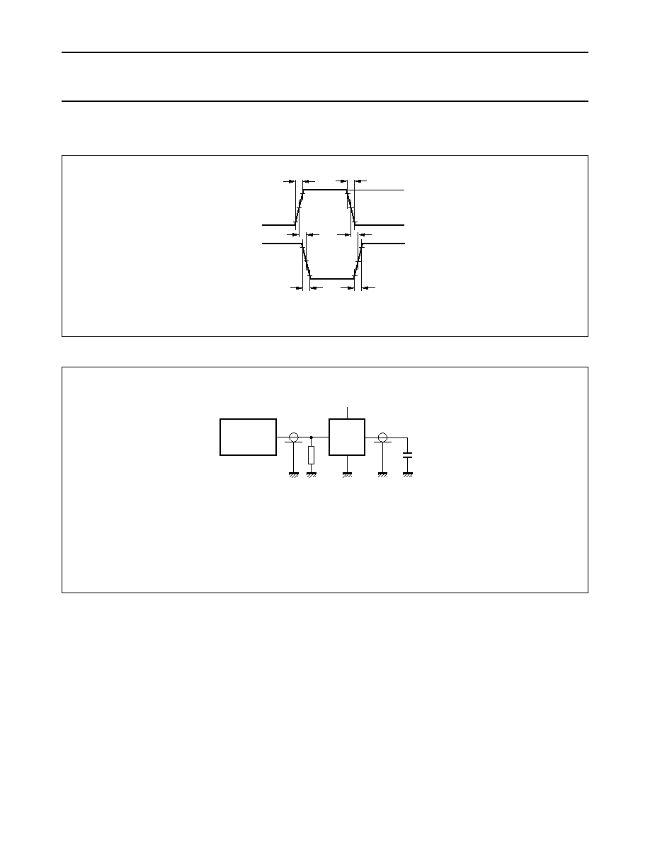
AC waveforms 74HCU
Test circuit for 74HCU
Fig.1 Input rise and fall times, transition times and propagation delays for combinatorial logic ICs.
handbook, halfpage
MGK564
10%
90%
90%
50%
50%
INPUT
OUTPUT
tr
tf
tPHL
tTHL
tPLH
tTLH
10%
GND
VCC
C
L
=
load capacitance including jig and probe capacitance
(see AC CHARACTERISTICS for values).
R
T
=
termination resistance should be equal to the output impedance Z
o
of
the pulse generator.
Fig.2 Test circuit.
handbook, halfpage
MGK565
PULSE
GENERATOR
D.U.T
VCC
VI
VO
RT
CL
50 pF
March 1988
10
Philips Semiconductors
HCMOS family characteristics
FAMILY SPECIFICATIONS
HC TYPES
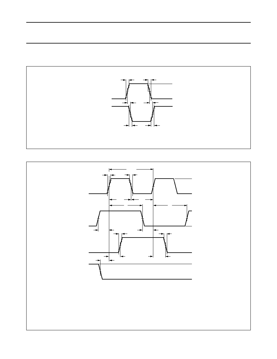
AC waveforms 74HC
AC waveforms 74HC
Fig.3 Input rise and fall times, transition times and propagation delays for combinatorial logic ICs.
handbook, halfpage
MGK564
10%
90%
90%
50%
50%
INPUT
OUTPUT
tr
tf
tPHL
tTHL
tPLH
tTLH
10%
GND
VCC
handbook, full pagewidth
MGK569
10 %
90%
50%
CLOCK
INPUT
VCC
GND
50%
DATA
INPUT
VCC
GND
10%
90%
50%
OUTPUT
tsu
tPHL
tPLH
tsu
tTLH
tTHL
50%
SET,
RESET,
PRESET
INPUT
VCC
GND
tr
tf
tWH
th
th
tWL
trem
1/fmax
Fig.4
Set-up times, hold times, removal times, propagation delays and the maximum clock pulse frequency for
sequential logic ICs.
(1) In Fig.4 the active transition of the clock is going from LOW-to-HIGH and the active level of the forcing signals (SET, RESET
and PRESET) is HIGH. The actual direction of the transition of the clock input and the actual active levels of the forcing signals
are specified in the individual device data sheet.
(2) For AC measurements: t
r
= t
f
= 6 ns; when measuring f
max
, there is no constraint on t
r
, t
f
with 50% duty factor.

March 1988
11
Philips Semiconductors
HCMOS family characteristics
FAMILY SPECIFICATIONS
Test circuit for 74HC
AC waveforms 74HC (continued)
C
L
=
load capacitance including jig and probe capacitance
(see AC CHARACTERISTICS for values).
R
T
=
termination resistance should be equal to the output impedance Z
o
of
the pulse generator.
Fig.5 Test circuit.
handbook, halfpage
MGK565
PULSE
GENERATOR
D.U.T
VCC
VI
VO
RT
CL
50 pF
Fig.6 Propagation delays of 3-state outputs.
handbook, full pagewidth
MGK562
tPLZ
tPHZ
outputs
disabled
outputs
enabled
90%
10%
10%
90%
50%
outputs
enabled
OUTPUT
LOW-to-OFF
OFF-to-LOW
OUTPUT
HIGH-to-OFF
OFF-to-HIGH
OUTPUT
ENABLE
VCC
GND
tPZL
tf
tr
tPZH
50%
50%

March 1988
12
Philips Semiconductors
HCMOS family characteristics
FAMILY SPECIFICATIONS
Test circuit for 74HC
HCT TYPES
AC waveforms 74HCT
handbook, full pagewidth
MGK563
D.U.T
VCC
VCC
VI
VO
RT
RL = 1 k
CL
50 pF
PULSE
GENERATOR
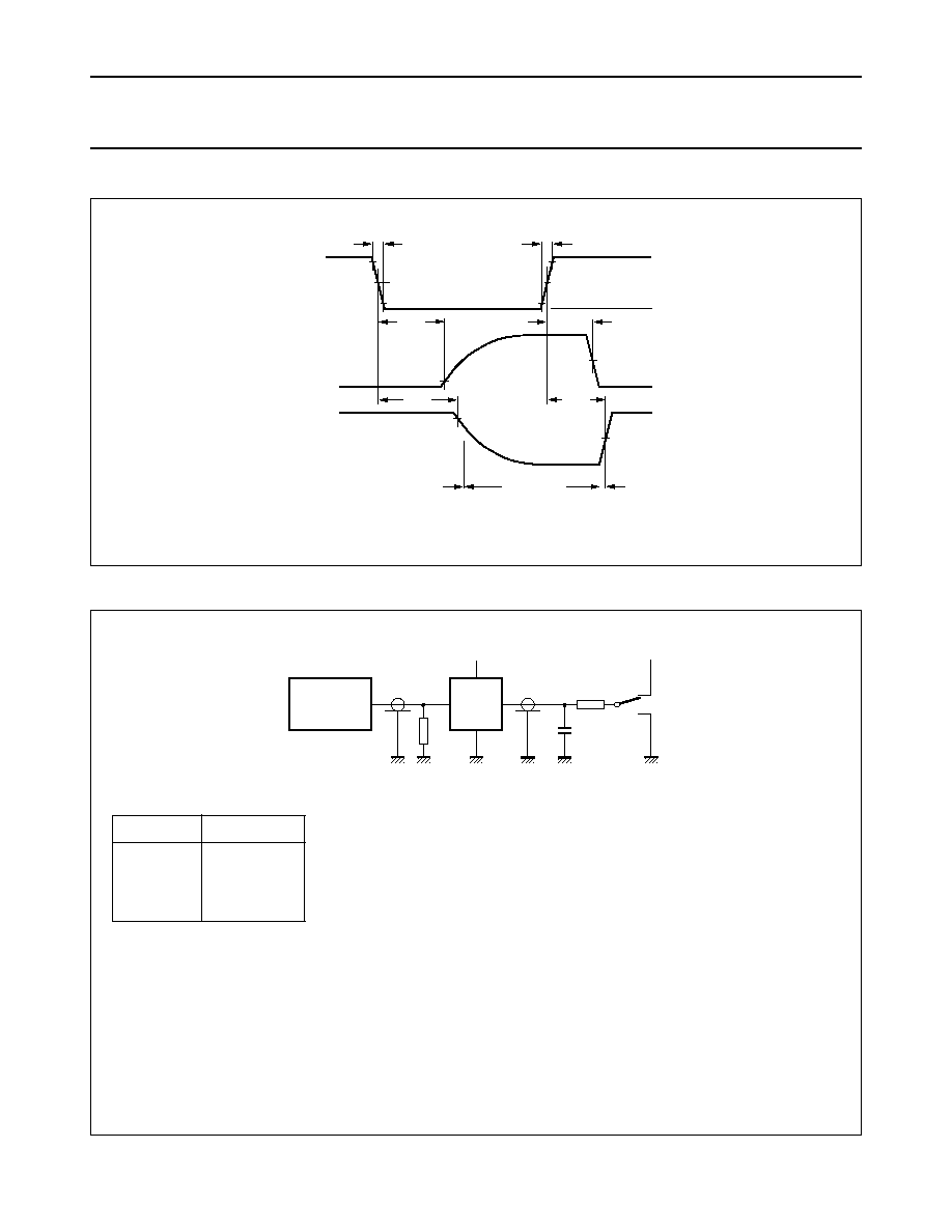
Switch position
Note
1. For open-drain N-channel outputs t
PLZ
and t
PZL
are applicable.
TEST
SWITCH
t
PZH
t
PZL
t
PHZ
t
PLZ
GND
V
CC
GND
V
CC
Fig.7 Test circuit for 3-state outputs.
C
L
=
load capacitance including jig and probe capacitance
(see AC CHARACTERISTICS for values).
R
T
=
termination resistance should be equal to the output impedance Z
o
of
the pulse generator.
Fig.8 Input rise and fall times, transition times and propagation delays for combinatorial logic ICs.
handbook, halfpage
MGK567
10%
90%
90%
1.3 V
1.3 V
INPUT
OUTPUT
tr
tf
tPHL
tTHL
tPLH
tTLH
10%
GND
3 V
March 1988
13
Philips Semiconductors
HCMOS family characteristics
FAMILY SPECIFICATIONS
AC waveforms 74HCT
Test circuit for 74HCT
handbook, full pagewidth
MGK568
10%
90%
1.3 V
CLOCK
INPUT
3 V
GND
1.3 V
DATA
INPUT
3 V
GND
10%
90%
1.3 V
OUTPUT
tsu
tPHL
tPLH
tsu
tTLH
tTHL
1.3 V
SET,
RESET,
PRESET
INPUT
3 V
GND
tr
tf
tWH
th
th
tWL
trem
1/fmax
Fig.9
Set-up times, hold times, removal times, propagation delays and the maximum clock pulse frequency for
sequential logic ICs.
(1) In Fig.9 the active transition of the clock is going from LOW-to-HIGH and the active level of the forcing signals
(SET, RESET and PRESET) is HIGH. The actual direction of the transition of the clock input and the actual
active levels of the forcing signals are specified in the individual device data sheet.
(2) For AC measurements: t
r
= t
f
= 6 ns; when measuring f
max
, there is no constraint on t
r
, t
f
with 50% duty factor.
handbook, halfpage
MGK565
PULSE
GENERATOR
D.U.T
VCC
VI
VO
RT
CL
50 pF
C
L
=
load capacitance including jig and probe capacitance (see AC
CHARACTERISTICS for values).
R
T
=
termination resistance should be equal to the output impedance Z
o
of
the pulse generator.
Fig.10 Test circuit.
March 1988
14
Philips Semiconductors
HCMOS family characteristics
FAMILY SPECIFICATIONS
AC waveforms 74HCT (continued)
Test circuit for 74HCT
Fig.11 Propagation delays of 3-state outputs.
handbook, full pagewidth
MGK566
tPLZ
tPHZ
outputs
disabled
outputs
enabled
90%
10%
10%
90%
1.3 V
outputs
enabled
OUTPUT
LOW-to-OFF
OFF-to-LOW
OUTPUT
HIGH-to-OFF
OFF-to-HIGH
OUTPUT
ENABLE
tPZL
tf
tr
tPZH
1.3 V
1.3 V
Switch position
Note
1. For open-drain N-channel outputs t
PLZ
and t
PZL
are applicable.
TEST
SWITCH
t
PZH
t
PZL
t
PHZ
t
PLZ
GND
V
CC
GND
V
CC
Fig.12 Test circuit for 3-state outputs.
C
L
=
load capacitance including jig and probe capacitance
(see AC CHARACTERISTICS for values).
R
T
=
termination resistance should be equal to the output impedance Z
o
of
the pulse generator.
handbook, full pagewidth
MGK563
D.U.T
VCC
VCC
VI
VO
RT
RL = 1 k
CL
50 pF
PULSE
GENERATOR

March 1988
15
Philips Semiconductors
HCMOS family characteristics
FAMILY SPECIFICATIONS
DATA SHEET SPECIFICATION GUIDE
INTRODUCTION
The 74HCMOS data sheets have been designed for
ease-of-use. A minimum of cross-referencing for more
information is needed.
TYPICAL PROPAGATION DELAY AND FREQUENCY
The typical propagation delays listed at the top of the data
sheets are the average of t
PLH
and t
PHL
for the longest data
path through the device with a 15 pF load.
For clocked devices, the maximum frequency of operation
is also given. The typical operating frequency is the
maximum device operating frequency with a 50% duty
factor and no constraints on t
r
and t
f
.
LOGIC SYMBOLS
Two logic symbols are given for each device - the
conventional one (Logic Symbol) which explicitly shows
the internal logic (except for complex logic) and the IEC
Logic Symbol as developed by the IEC (International
Electrotechnical Commission).
The IEC has been developing a very powerful symbolic
language that can show the relationship of each input of a
digital logic current to each output without explicitly
showing the internal logic.
Internationally, Working Group 2 of IEC Technical
Committee TC-3 has prepared a new document
(Publication 617-12) which supersedes
Publication 117-15, published in 1972.
RATINGS
The "RATINGS" table (Limiting values in accordance with
the Absolute Maximum System - IEC134) lists the
maximum limits to which the device can be subjected
without damage. This doesn't imply that the device will
function at these extreme conditions, only that, when these
conditions are removed and the device operated within the
Recommended Operating Conditions, it will still be
functional and its useful life won't have been shortened.
The maximum rated supply voltage of 7 V is well below the
typical breakdown voltage of 18 V.
RECOMMENDED OPERATING CONDITIONS
The "RECOMMENDED OPERATING CONDITIONS"
table lists the operating ambient temperature and the
conditions under which the limits in the "DC
CHARACTERISTICS" and "AC CHARACTERISTICS"
tables will be met. The table should not be seen as a set of
limits guaranteed by the manufacturer, but as the
conditions used to test the devices and guarantee that
they will then meet the limits in the DC and AC
CHARACTERISTICS tables.
DC CHARACTERISTICS
The "DC CHARACTERISTICS" table reflects the DC limits
used during testing. The values published are guaranteed.
The threshold values of V
IH
and V
IL
can be tested by the
user. If V
IH
and V
IL
are applied to the inputs, the output
voltages will be those published in the "DC
CHARACTERISTICS" table. There is a tendency, by
some, to use the published V
IH
and V
IL
thresholds to test a
device for functionality in a "function-table exercizer"
mode. This frequently causes problems because of the
noise present at the test head of automated test
equipment with cables up to 1 metre. Parametric tests,
such as those used for the output levels under the V
IH
and
V
IL
conditions are done fairly slowly, in the order of
milliseconds, so that there is no noise at the inputs when
the outputs are measured. But in functionality testing, the
outputs are measured much faster, so there can be noise
on the inputs, before the device has assumed its final and
correct output state. Thus, never use V
IH
and V
IL
to test the
functionality of any HCMOS device type; instead, use input
voltages of V
CC
(for the HIGH state) and 0 V (for the LOW
state). In no way does this imply that the devices are
noise-sensitive in the final system.
In the data sheets, it may appear strange that the typical
V
IL
is higher than the maximum V
IL
. However, this is
because V
ILmax
is the maximum V
IL
(guaranteed) for all
devices that will be recognized as a logic LOW. However,
typically a higher V
IL
will also be recognized as a logic
LOW. Conversely, the typical V
IH
is lower than its minimum
guaranteed level.
For 74HCMOS, unlike TTL, no output HIGH short-circuit
current is specified. The use of this current, for example, to
calculate propagation delays with capacitive loads, is
covered by the HCMOS graphs showing the output drive
capability and those showing the dependence of
propagation delay on load capacitance.
The quiescent supply current I
CC
is the leakage current of
all the reversed-biased diodes and the OFF-state MOS
transistors. It is measured with the inputs at V
CC
or GND
and is typically a few nA.

March 1988
16
Philips Semiconductors
HCMOS family characteristics
FAMILY SPECIFICATIONS
AC CHARACTERISTICS
The "AC CHARACTERISTICS" table lists the guaranteed
limits when a device is tested under the conditions given in
the AC Test Circuits and Waveforms section.
TEST CIRCUITS
Good high-frequency wiring practices should be used in
test circuits. Capacitor leads should be as short as
possible to minimize ripples on the output waveform
transitions and undershoot. Generous ground metal
(preferably a ground-plane) should be used for the same
reasons. A V
CC
decoupling capacitor should be provided
at the test socket, also with short leads. Input signals
should have rise and fall times of 6 ns, a signal swing of
0 V to V
CC
for 74HC and 0 V to 3 V for 74HCT; a 1.0 MHz
square wave is recommended for most propagation delay
tests. The repetition rate must be increased for testing
f
max
. Two pulse generators are usually required for testing
such parameters as set-up time, hold time and removal
time. f
max
is also tested with 6 ns input rise and fall times,
with a 50% duty factor, but for typical f
max
as high as
60 MHz, there are no constraints on rise and fall times.

March 1988
17
Philips Semiconductors
HCMOS family characteristics
FAMILY SPECIFICATIONS
DEFINITIONS OF SYMBOLS AND TERMS USED IN
HCMOS DATA SHEETS
Currents
Positive current is defined as conventional current flow
into a device.
Negative current is defined as conventional current flow
out of a device.
Voltages
All voltages are referenced to GND (ground), which is
typically 0 V.
I
CC
Quiescent power supply current; the current
flowing into the V
CC
supply terminal.
I
CC
Additional quiescent supply current per input
pin at a specified input voltage and V
CC
.
I
GND
Quiescent power supply current; the current
flowing into the GND terminal.
I
I
Input leakage current; the current flowing into a
device at a specified input voltage and V
CC
.
I
IK
Input diode current; the current flowing into a
device at a specified input voltage.
I
O
Output source or sink current: the current
flowing into a device at a specified output
voltage.
I
OK
Output diode current; the current flowing into a
device at a specified output voltage.
I
OZ
OFF-state output current; the leakage current
flowing into the output of a 3-state device in the
OFF-state, when the output is connected to
V
CC
or GND.
I
S
Analog switch leakage current; the current
flowing into an analog switch at a specified
voltage across the switch and V
CC
.
GND
Supply voltage; for a device with a single
negative power supply, the most negative
power supply, used as the reference level for
other voltages; typically ground.
V
CC
Supply voltage; the most positive potential on
the device.
V
EE
Supply voltage; one of two (GND and V
EE
)
negative power supplies.
V
H
Hysteresis voltage; difference between the
trigger levels, when applying a positive and a
negative-going input signal.
V
IH
HIGH level input voltage; the range of input
voltages that represents a logic HIGH level in
the system.
Analog terms
Capacitances
V
IL
LOW level input voltage; the range of input
voltages that represents a logic LOW level in
the system.
V
OH
HIGH level output voltage; the range of
voltages at an output terminal with a specified
output loading and supply voltage. Device
inputs are conditioned to establish a HIGH level
at the output.
V
OL
LOW level output voltage; the range of voltages
at an output terminal with a specified output
loading and supply voltage. Device inputs are
conditioned to establish a LOW level at the
output.
V
T
+
Trigger threshold voltage; positive-going signal.
V
T
-
Trigger threshold voltage; negative-going
signal.
R
ON
ON-resistance; the effective ON-state
resistance of an analog switch, at a specified
voltage across the switch and output load.
R
ON
ON-resistance; the difference in
ON-resistance between any two switches of an
analog device at a specified voltage across the
switch and output load.
C
I
Input capacitance; the capacitance measured
at a terminal connected to an input of a device.
C
I/O
Input/Output capacitance; the capacitance
measured at a terminal connected to an I/O-pin
(e.g. a transceiver).
C
L
Output load capacitance; the capacitance
connected to an output terminal including jig
and probe capacitance.
C
PD
Power dissipation capacitance; the capacitance
used to determine the dynamic power
dissipation per logic function, when no extra
load is provided to the device.
C
S
Switch capacitance; the capacitance of a
terminal to a switch of an analog device.

March 1988
18
Philips Semiconductors
HCMOS family characteristics
FAMILY SPECIFICATIONS
AC switching parameters
f
i
Input frequency; for combinatorial logic devices
the maximum number of inputs and outputs
switching in accordance with the device
function table. For sequential logic devices the
clock frequency using alternate HIGH and LOW
for data input or using the toggle mode,
whichever is applicable.
f
o
Output frequency; each output.
f
max
Maximum clock frequency; clock input
waveforms should have a 50% duty factor and
be such as to cause the outputs to be switching
from 10%V
CC
to 90%V
CC
in accordance with
the device function table.
t
h
Hold time; the interval immediately following the
active transition of the timing pulse (usually the
clock pulse) or following the transition of the
control input to its latching level, during which
interval the data to be recognized must be
maintained at the input to ensure their
continued recognition. A negative hold time
indicates that the correct logic level may be
released prior to the timing pulse and still be
recognized.
t
r
,
t
f
Clock input rise and fall times; 10% and 90%
values.
t
PHL
Propagation delay; the time between the
specified reference points, normally the 50%
points for 74HC and 74HCU devices on the
input and output waveforms and the 1.3 V
points for the 74HCT devices, with the output
changing from the defined HIGH level to the
defined LOW level.
t
PLH
Propagation delay; the time between the
specified reference points, normally the 50%
points for 74HC and 74HCU devices on the
input and output waveforms and the 1.3 V point
for the 74HCT devices, with the output
changing from the defined LOW level to the
defined HIGH level.
t
PHZ
3-state output disable time; the time between
the specified reference points, normally the
50% points for the 74HC and 74HCU devices
and the 1.3 V points for the 74HCT devices on
the output enable input voltage waveform and a
point representing 10% of the output swing on
the output voltage waveform of a 3-state
device, with the output changing from
a HIGH level (V
OH
) to a high impedance
OFF-state (Z).
t
PLZ
3-state output disable time; the time between
the specified reference points, normally the
50% points for the 74HC devices and the 1.3 V
points for the 74HCT devices on the output
enable input voltage waveform and a point
representing 10% of the output swing on the
output voltage waveform of a 3-state
device, with the output changing from a LOW
level (V
OL
) to a high impedance OFF-state (Z).
t
PZH
3-state output enable time; the time between
the specified reference points, normally the
50% points for the 74HC devices and 1.3 V
points for the 74HCT devices on the output
enable input voltage waveform and the 50%
point on the output voltage waveform of a
3-state device, with the output changing from a
high impedance OFF-state (Z) to a HIGH level
(V
OH
).
t
PZL
3-state output enable time; the time between
the specified reference points, normally the
50% points for the 74HC devices and the 1.3 V
points for the 74HCT devices on the output
enable input voltage waveform and the 50%
point on the output voltage waveform of a
3-state device, with the output changing from a
high impedance OFF-state (Z) to a LOW level
(V
OL
).
t
rem
Removal time; the time between the end of an
overriding asynchronous input, typically a clear
or reset input, and the earliest permissible
beginning of a synchronous control input,
typically a clock input, normally measured at
the 50% points for 74HC devices and the 1.3 V
points for the 74HCT devices on both input
voltage waveforms.
t
su
Set-up time; the interval immediately preceding
the active transition of the timing pulse (usually
the clock pulse) or preceding the transition of
the control input to its latching level, during
which interval the data to be recognized must
be maintained at the input to ensure their
recognition. A negative set-up time indicates
that the correct logic level may be initiated
sometime after the active transition of the
timing pulse and still be recognized.

March 1988
19
Philips Semiconductors
HCMOS family characteristics
FAMILY SPECIFICATIONS
t
THL
Output transition time; the time between two
specified reference points on a waveform,
normally 90% and 10% points, that is changing
from HIGH-to-LOW.
t
THL
Output transition time; the time between two
specified reference points on a waveform,
normally 10% and 90% points, that is changing
from LOW-to-HIGH.
t
W
Pulse width; the time between the 50%
amplitude points on the leading and trailing
edges of a pulse for 74HC and 74HCU devices
and at the 1.3 V points for 74HCT devices.