 | –≠–ª–µ–∫—Ç—Ä–æ–Ω–Ω—ã–π –∫–æ–º–ø–æ–Ω–µ–Ω—Ç: 74HCT109 | –°–∫–∞—á–∞—Ç—å:  PDF PDF  ZIP ZIP |
DATA SHEET
Product specification
Supersedes data of December 1990
File under Integrated Circuits, IC06
1997 Nov 25
INTEGRATED CIRCUITS
74HC/HCT109
Dual JK flip-flop with set and reset;
positive-edge trigger
For a complete data sheet, please also download:
∑
The IC06 74HC/HCT/HCU/HCMOS Logic Family Specifications
∑
The IC06 74HC/HCT/HCU/HCMOS Logic Package Information
∑
The IC06 74HC/HCT/HCU/HCMOS Logic Package Outlines
1997 Nov 25
2
Philips Semiconductors
Product specification
Dual JK flip-flop with set and reset;
positive-edge trigger
74HC/HCT109
FEATURES
∑
J, K inputs for easy D-type flip-flop
∑
Toggle flip-flop or "do nothing" mode
∑
Output capability: standard
∑
I
CC
category: flip-flops
GENERAL DESCRIPTION
The 74HC/HCT109 are high-speed Si-gate CMOS devices
and are pin compatible with low power Schottky TTL
(LSTTL). They are specified in compliance with JEDEC
standard no. 7A.
The 74HC/HCT109 are dual positive-edge triggered, JK
flip-flops with individual J, K inputs, clock (CP) inputs, set
(S
D
) and reset (R
D
) inputs; also complementary Q and Q
outputs.
The set and reset are asynchronous active LOW inputs
and operate independently of the clock input.
The J and K inputs control the state changes of the
flip-flops as described in the mode select function table.
The J and K inputs must be stable one set-up time prior to
the LOW-to-HIGH clock transition for predictable
operation.
The JK design allows operation as a D-type flip-flop by
tying the J and K inputs together.
Schmitt-trigger action in the clock input makes the circuit
highly tolerant to slower clock rise and fall times.
QUICK REFERENCE DATA
GND = 0 V; T
amb
= 25
∞
C; t
r
= t
f
= 6 ns
Notes
1. C
PD
is used to determine the dynamic power dissipation (P
D
in
µ
W):
P
D
= C
PD
◊
V
CC
2
◊
f
i
+
(C
L
◊
V
CC
2
◊
f
o
) where:
f
i
= input frequency in MHz
f
o
= output frequency in MHz
(C
L
◊
V
CC
2
◊
f
o
) = sum of outputs
C
L
= output load capacitance in pF
V
CC
= supply voltage in V
2. For HC the condition is V
I
= GND to V
CC
For HCT the condition is V
I
= GND to V
CC
-
1.5 V.
ORDERING INFORMATION
See
"74HC/HCT/HCU/HCMOS Logic Package Information"
.
SYMBOL
PARAMETER
CONDITIONS
TYPICAL
UNIT
HC
HCT
t
PHL
/ t
PLH
propagation delay
C
L
= 15 pF;
V
CC
= 5 V
nCP to nQ, nQ
15
17
ns
nS
D
to nQ, nQ
12
14
ns
nR
D
to nQ, nQ
12
15
ns
f
max
maximum clock frequency
75
61
MHz
C
I
input capacitance
3.5
3.5
pF
C
PD
power dissipation
capacitance per flip-flop
notes 1 and 2
20
22
pF

1997 Nov 25
3
Philips Semiconductors
Product specification
Dual JK flip-flop with set and reset;
positive-edge trigger
74HC/HCT109
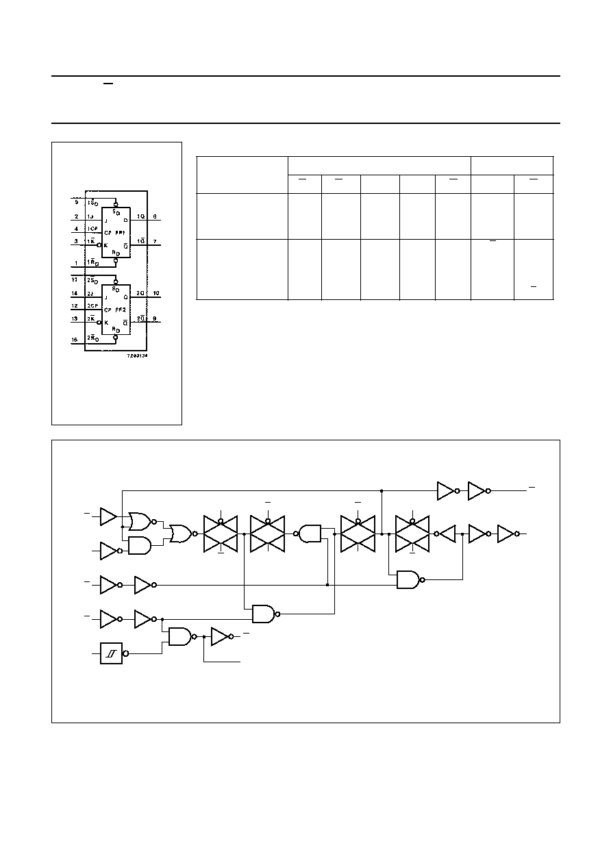
PIN DESCRIPTION
PIN NO.
SYMBOL
NAME AND FUNCTION
1, 15
1R
D
, 2R
D
asynchronous reset-direct input (active LOW)
2, 14, 3, 13
1J, 2J, 1K, 2K
synchronous inputs; flip-flops 1 and 2
4, 12
1CP, 2CP
clock input (LOW-to-HIGH, edge-triggered)
5, 11
1S
D
, 2S
D
asynchronous set-direct input (active LOW)
6, 10
1Q, 2Q
true flip-flop outputs
7, 9
1Q, 2Q
complement flip-flop outputs
8
GND
ground (0 V)
16
V
CC
positive supply voltage
Fig.1 Pin configuration.
Fig.2 Logic symbol.
Fig.3 IEC logic symbol.
1997 Nov 25
4
Philips Semiconductors
Product specification
Dual JK flip-flop with set and reset;
positive-edge trigger
74HC/HCT109
Fig.4 Functional diagram.
FUNCTION TABLE
Notes
1. H = HIGH voltage level
h = HIGH voltage level one set-up time prior to the LOW-to-HIGH CP transition
L = LOW voltage level
I = LOW voltage level one set-up time prior to the LOW-to-HIGH CP transition
q = lower case letters indicate the state of the referenced output one set-up time
prior to the LOW-to-HIGH CP transition
X = don't care
= LOW-to-HIGH CP transition
OPERATING
MODE
INPUTS
OUTPUTS
S
D
R
D
CP
J
K
Q
Q
asynchronous set
L
H
X
X
X
H
L
asynchronous reset
H
L
X
X
X
L
H
undetermined
L
L
X
X
X
H
H
toggle
H
H
h
l
q
q
load "0" (reset)
H
H
l
l
L
H
load "1" (set)
H
H
h
h
H
L
hold "no change"
H
H
l
h
q
q
PACKAGE OUTLINES
See
"74HC/HCT/HCU/HCMOS Logic Package Outlines"
.
Fig.5 Logic diagram (one flip-flop).
handbook, full pagewidth
MBK217
C
C
C
C
C
K
J
CP
S
R
C
C
C
C
C
Q
Q

1997 Nov 25
5
Philips Semiconductors
Product specification
Dual JK flip-flop with set and reset;
positive-edge trigger
74HC/HCT109
DC CHARACTERISTICS FOR 74HC
For the DC characteristics see
"74HC/HCT/HCU/HCMOS Logic Family Specifications"
.
Output capability: standard
I
CC
category: flip-flops
AC CHARACTERISTICS FOR 74HC
GND = 0 V; t
r
= t
f
= 6 ns; C
L
= 50 pF
SYMBOL
PARAMETER
T
amb
(
∞
C)
TEST CONDITIONS
74HC
UNIT
V
CC
(V)
WAVEFORMS
+
25
-
40 to
+
85
-
40 to
+
125
min.
typ.
max.
min.
max.
min.
max.
t
PHL
/ t
PLH
propagation delay
nCP to nQ, nQ
50
18
14
175
35
30
220
44
37
265
53
45
ns
2.0
4.5
6.0
Fig.6
t
PLH
propagation delay
nS
D
to nQ
30
11
9
120
24
20
150
30
26
180
36
31
ns
2.0
4.5
6.0
Fig.7
t
PHL
propagation delay
nS
D
to nQ
41
15
12
155
31
26
195
39
33
235
47
40
ns
2.0
4.5
6.0
Fig.7
t
PHL
propagation delay
nR
D
to nQ
41
15
12
185
37
31
230
46
39
280
56
48
ns
2.0
4.5
6.0
Fig.7
t
PLH
propagation delay
nR
D
to nQ
39
14
11
170
34
29
215
43
37
255
51
43
ns
2.0
4.5
6.0
Fig.7
t
THL
/ t
TLH
output transition
time
19
7
6
75
15
13
95
19
16
110
22
19
ns
2.0
4.5
6.0
Fig.6
t
W
clock pulse width
HIGH or LOW
80
16
14
19
7
6
100
20
17
120
24
20
ns
2.0
4.5
6.0
Fig.6
t
W
set or reset pulse
width HIGH or LOW
80
16
14
14
5
4
100
20
17
120
24
20
ns
2.0
4.5
6.0
Fig.7
t
rem
removal time
nS
D
, nR
D
to nCP
70
14
12
19
7
6
90
18
15
105
21
18
ns
2.0
4.5
6.0
Fig.7
t
su
set-up time
nJ, nK to nCP
70
14
12
17
6
5
90
18
15
105
21
18
ns
2.0
4.5
6.0
Fig.6
t
h
hold time
nJ, nK to nCP
5
5
5
0
0
0
5
5
5
5
5
5
ns
2.0
4.5
6.0
Fig.6
f
max
maximum clock
pulse frequency
6.0
30
35
22
68
81
5.0
24
28
4.0
20
24
MHz
2.0
4.5
6.0
Fig.6