
DATA SHEET
Product specification
File under Integrated Circuits, IC06
September 1993
INTEGRATED CIRCUITS
74HC/HCT138
3-to-8 line decoder/demultiplexer;
inverting
For a complete data sheet, please also download:
∑
The IC06 74HC/HCT/HCU/HCMOS Logic Family Specifications
∑
The IC06 74HC/HCT/HCU/HCMOS Logic Package Information
∑
The IC06 74HC/HCT/HCU/HCMOS Logic Package Outlines
September 1993
2
Philips Semiconductors
Product specification
3-to-8 line decoder/demultiplexer; inverting
74HC/HCT138
FEATURES
∑
Demultiplexing capability
∑
Multiple input enable for easy expansion
∑
Ideal for memory chip select decoding
∑
Active LOW mutually exclusive outputs
∑
Output capability: standard
∑
I
CC
category: MSI
GENERAL DESCRIPTION
The 74HC/HCT138 are high-speed Si-gate CMOS devices
and are pin compatible with low power Schottky TTL
(LSTTL). They are specified in compliance with JEDEC
standard no. 7A.
The 74HC/HCT138 decoders accept three binary
weighted address inputs (A
0
, A
1
, A
2
) and when enabled,
provide 8 mutually exclusive active LOW outputs (Y
0
to
Y
7
).
The "138" features three enable inputs: two active LOW
(E
1
and E
2
) and one active HIGH (E
3
). Every output will be
HIGH unless E
1
and E
2
are LOW and E
3
is HIGH.
This multiple enable function allows easy parallel
expansion of the "138" to a 1-of-32 (5 lines to 32 lines)
decoder with just four "138" ICs and one inverter.
The "138" can be used as an eight output demultiplexer by
using one of the active LOW enable inputs as the data
input and the remaining enable inputs as strobes. Unused
enable inputs must be permanently tied to their
appropriate active HIGH or LOW state.
The "138" is identical to the "238" but has inverting outputs.
QUICK REFERENCE DATA
GND = 0 V; T
amb
= 25
∞
C; t
r
= t
f
= 6 ns
Notes
1. C
PD
is used to determine the dynamic power dissipation (P
D
in
µ
W):
P
D
= C
PD
◊
V
CC
2
◊
f
i
+
(C
L
◊
V
CC
2
◊
f
o
) where:
f
i
= input frequency in MHz
f
o
= output frequency in MHz
(C
L
◊
V
CC
2
◊
f
o
) = sum of outputs
C
L
= output load capacitance in pF
V
CC
= supply voltage in V
2. For HC the condition is V
I
= GND to V
CC
For HCT the condition is V
I
= GND to V
CC
-
1.5 V
ORDERING INFORMATION
See
"74HC/HCT/HCU/HCMOS Logic Package Information"
.
SYMBOL
PARAMETER
CONDITIONS
TYPICAL
UNIT
HC
HCT
propagation delay
C
L
= 15 pF; V
CC
= 5 V
t
PHL
/ t
PLH
A
n
to Y
n
12
17
ns
t
PHL
/ t
PLH
E
3
to Y
n
E
n
to Y
n
14
19
ns
C
I
input capacitance
3.5
3.5
pF
C
PD
power dissipation capacitance per package
notes 1 and 2
67
67
pF
September 1993
3
Philips Semiconductors
Product specification
3-to-8 line decoder/demultiplexer; inverting
74HC/HCT138
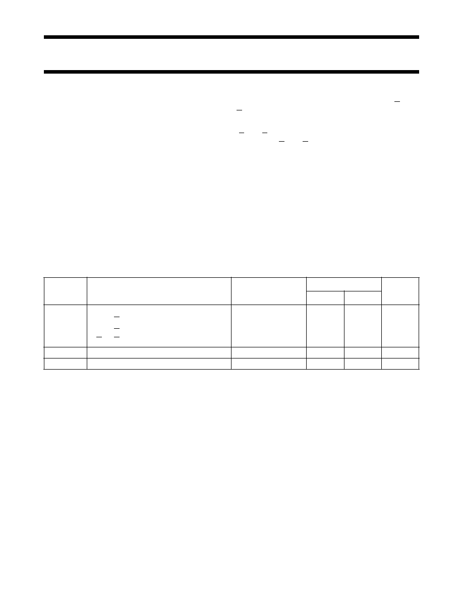
PIN DESCRIPTION
PIN NO.
SYMBOL
NAME AND FUNCTION
1, 2, 3
A
0
to A
2
address inputs
4, 5
E
1
, E
2
enable inputs (active LOW)
6
E
3
enable input (active HIGH)
8
GND
ground (0 V)
15, 14, 13, 12, 11, 10, 9, 7
Y
0
to Y
7
outputs (active LOW)
16
V
CC
positive supply voltage
Fig.1 Pin configuration.
Fig.2 Logic symbol.
handbook, halfpage
MLB312
A 0
A 1
A 2
1
2
3
15
13
11
7
9
10
12
14
Y0
Y1
Y2
Y3
Y4
Y5
Y6
Y7
4
5
6
E1
E2
E3
Fig.3 IEC logic symbol.
(a)
(b)
Fig.4 Functional diagram.
September 1993
4
Philips Semiconductors
Product specification
3-to-8 line decoder/demultiplexer; inverting
74HC/HCT138
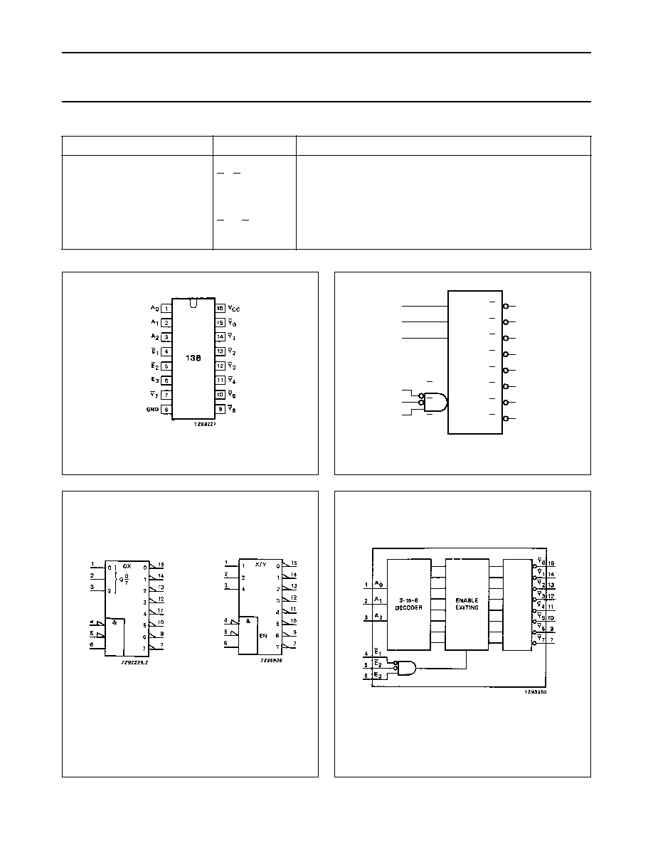
FUNCTION TABLE
Notes
1. H = HIGH voltage level
L = LOW voltage level
X = don't care
INPUTS
OUTPUTS
E
1
E
2
E
3
A
0
A
1
A
2
Y
0
Y
1
Y
2
Y
3
Y
4
Y
5
Y
6
Y
7
H
X
X
X
H
X
X
X
L
X
X
X
X
X
X
X
X
X
H
H
H
H
H
H
H
H
H
H
H
H
H
H
H
H
H
H
H
H
H
H
H
H
L
L
L
L
L
L
L
L
H
H
H
H
L
H
L
H
L
L
H
H
L
L
L
L
L
H
H
H
H
L
H
H
H
H
L
H
H
H
H
L
H
H
H
H
H
H
H
H
H
H
H
H
H
H
H
H
L
L
L
L
L
L
L
L
H
H
H
H
L
H
L
H
L
L
H
H
H
H
H
H
H
H
H
H
H
H
H
H
H
H
H
H
H
H
H
H
L
H
H
H
H
L
H
H
H
H
L
H
H
H
H
L
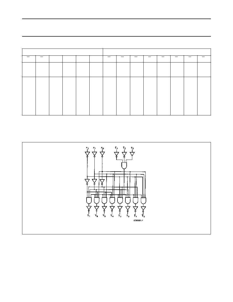
Fig.5 Logic diagram.

September 1993
5
Philips Semiconductors
Product specification
3-to-8 line decoder/demultiplexer; inverting
74HC/HCT138
DC CHARACTERISTICS FOR 74HC
For the DC characteristics see
"74HC/HCT/HCU/HCMOS Logic Family Specifications"
.
Output capability: standard
I
CC
category: MSI
AC CHARACTERISTICS FOR 74HC
GND = 0 V; t
r
= t
f
= 6 ns; C
L
= 50 pF
SYMBOL
PARAMETER
T
amb
(
∞
C)
UNIT
TEST CONDITIONS
74HC
V
CC
(V)
WAVEFORMS
+
25
-
40 to
+
85
-
40 to
+
125
min.
typ.
max.
min.
max.
min.
max.
t
PHL
/ t
PLH
propagation delay
A
n
to Y
n
41
15
12
150
30
26
190
38
33
225
45
38
ns
2.0
4.5
6.0
Fig.6
t
PHL
/ t
PLH
propagation delay
E
3
to Y
n
47
17
14
150
30
26
190
38
33
225
45
38
ns
2.0
4.5
6.0
Fig.6
t
PHL
/ t
PLH
propagation delay
E
n
to Y
n
47
17
14
150
30
26
190
38
33
225
45
38
ns
2.0
4.5
6.0
Fig.7
t
THL
/ t
TLH
output transition
time
19
7
6
75
15
13
95
19
16
110
22
19
ns
2.0
4.5
6.0
Figs 6 and 7

September 1993
6
Philips Semiconductors
Product specification
3-to-8 line decoder/demultiplexer; inverting
74HC/HCT138
DC CHARACTERISTICS FOR 74HCT
For the DC characteristics see
"74HC/HCT/HCU/HCMOS Logic Family Specifications"
.
Output capability: standard
I
CC
category: MSI
Note to HCT types
The value of additional quiescent supply current (
I
CC
) for a unit load of 1 is given in the family specifications. To
determine
I
CC
per input, multiply this value by the unit load coefficient shown in the table below.
AC CHARACTERISTICS FOR 74HCT
GND = 0 V; t
r
= t
f
= 6 ns; C
L
= 50 pF
INPUT
UNIT LOAD COEFFICIENT
A
n
1.50
E
n
1.25
E
3
1.00
SYMBOL
PARAMETER
T
amb
(
∞
C)
UNIT
TEST CONDITIONS
74HCT
V
CC
(V)
WAVEFORMS
+
25
-
40 to
+
85
-
40 to
+
125
min.
typ.
max.
min.
max.
min.
max.
t
PHL
/ t
PLH
propagation delay
A
n
to Y
n
20
35
44
53
ns
4.5
Fig.6
t
PHL
/ t
PLH
propagation delay
E
3
to Y
n
18
40
50
60
ns
4.5
Fig.6
t
PHL
/ t
PLH
propagation delay
E
n
to Y
n
19
40
50
60
ns
4.5
Fig.7
t
THL
/ t
TLH
output transition
time
7
15
19
22
ns
4.5
Figs 6 and 7

September 1993
7
Philips Semiconductors
Product specification
3-to-8 line decoder/demultiplexer; inverting
74HC/HCT138
AC WAVEFORMS
PACKAGE OUTLINES
See
"74HC/HCT/HCU/HCMOS Logic Package Outlines"
.
Fig.6
Waveforms showing the address input (A
n
) and enable input (E
3
) to output (Y
n
) propagation delays and
the output transition times.
(1) HC : V
M
= 50%; V
I
= GND to V
CC
.
HCT: V
M
= 1.3 V; V
I
= GND to 3 V.
Fig.7
Waveforms showing the enable input (E
n
) to output (Y
n
) propagation delays and the output transition
times.
(1) HC : V
M
= 50%; V
I
= GND to V
CC
.
HCT: V
M
= 1.3 V; V
I
= GND to 3 V.