2003 Oct 30
2
Philips Semiconductors
Product specification
Hex inverting Schmitt trigger
74HC14; 74HCT14
FEATURES
∑
Applications:
≠ Wave and pulse shapers
≠ Astable multivibrators
≠ Monostable multivibrators.
∑
Complies with JEDEC standard no. 7A
∑
ESD protection:
HBM EIA/JESD22-A114-A exceeds 2000 V
MM EIA/JESD22-A115-A exceeds 200 V.
∑
Specified from
-
40 to +85
∞
C and
-
40 to +125
∞
C.
DESCRIPTION
The 74HC14 and 74HCT14 are high-speed Si-gate CMOS
devices and are pin compatible with low power Schottky
TTL (LSTTL). They are specified in compliance with
JEDEC standard no. 7A.
The 74HC14 and 74HCT14 provide six inverting buffers
with Schmitt-trigger action. They are capable of
transforming slowly changing input signals into sharply
defined, jitter-free output signals.
QUICK REFERENCE DATA
GND = 0 V; T
amb
= 25
∞
C; t
r
= t
f
= 6 ns
Notes
1. C
PD
is used to determine the dynamic power dissipation (P
D
in
µ
W):
P
D
= C
PD
◊
V
CC
2
◊
f
i
◊
N +
(C
L
◊
V
CC
2
◊
f
o
) where:
f
i
= input frequency in MHz;
f
o
= output frequency in MHz;
C
L
= output load capacitance in pF;
V
CC
= supply voltage in Volts;
N = total load switching outputs;
(C
L
◊
V
CC
2
◊
f
o
) = sum of the outputs.
2. For type 74HC14 the condition is V
I
= GND to V
CC
.
For type 74HCT14 the condition is V
I
= GND to V
CC
-
1.5 V.
SYMBOL
PARAMETER
CONDITIONS
TYPICAL
UNIT
HC
HCT
t
PHL
/t
PLH
propagation delay nA to nY
C
L
= 15 pF; V
CC
= 5 V 12
17
ns
C
I
input capacitance
3.5
3.5
pF
C
PD
power dissipation capacitance per gate notes 1 and 2
7
8
pF
2003 Oct 30
4
Philips Semiconductors
Product specification
Hex inverting Schmitt trigger
74HC14; 74HCT14
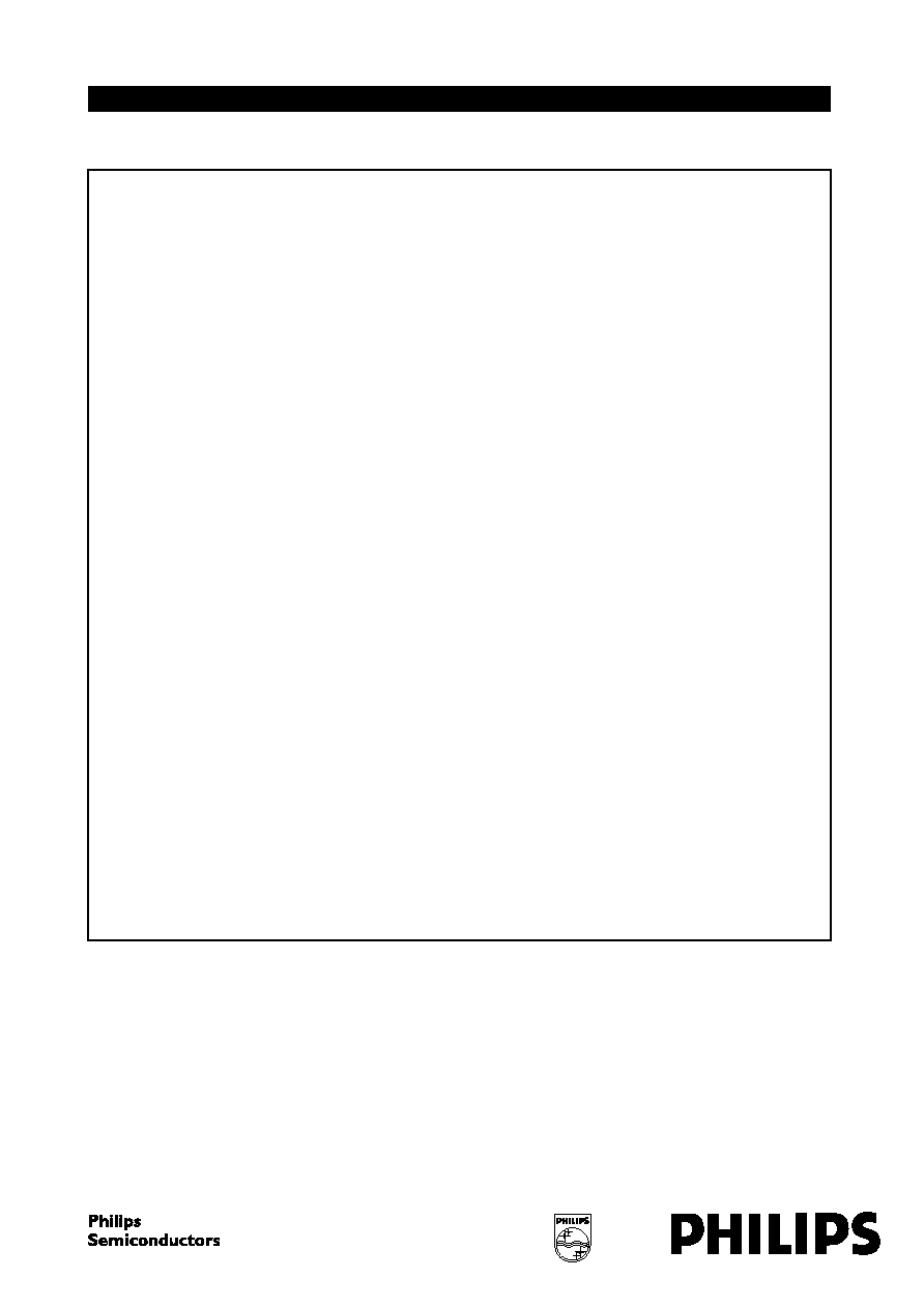
handbook, halfpage
MNA839
14
1
2
3
4
5
6
7
8
14
13
12
11
10
9
1A
1Y
2A
2Y
3A
3Y
GND
4Y
4A
5Y
5A
6Y
6A
VCC
Fig.1 Pin configuration.
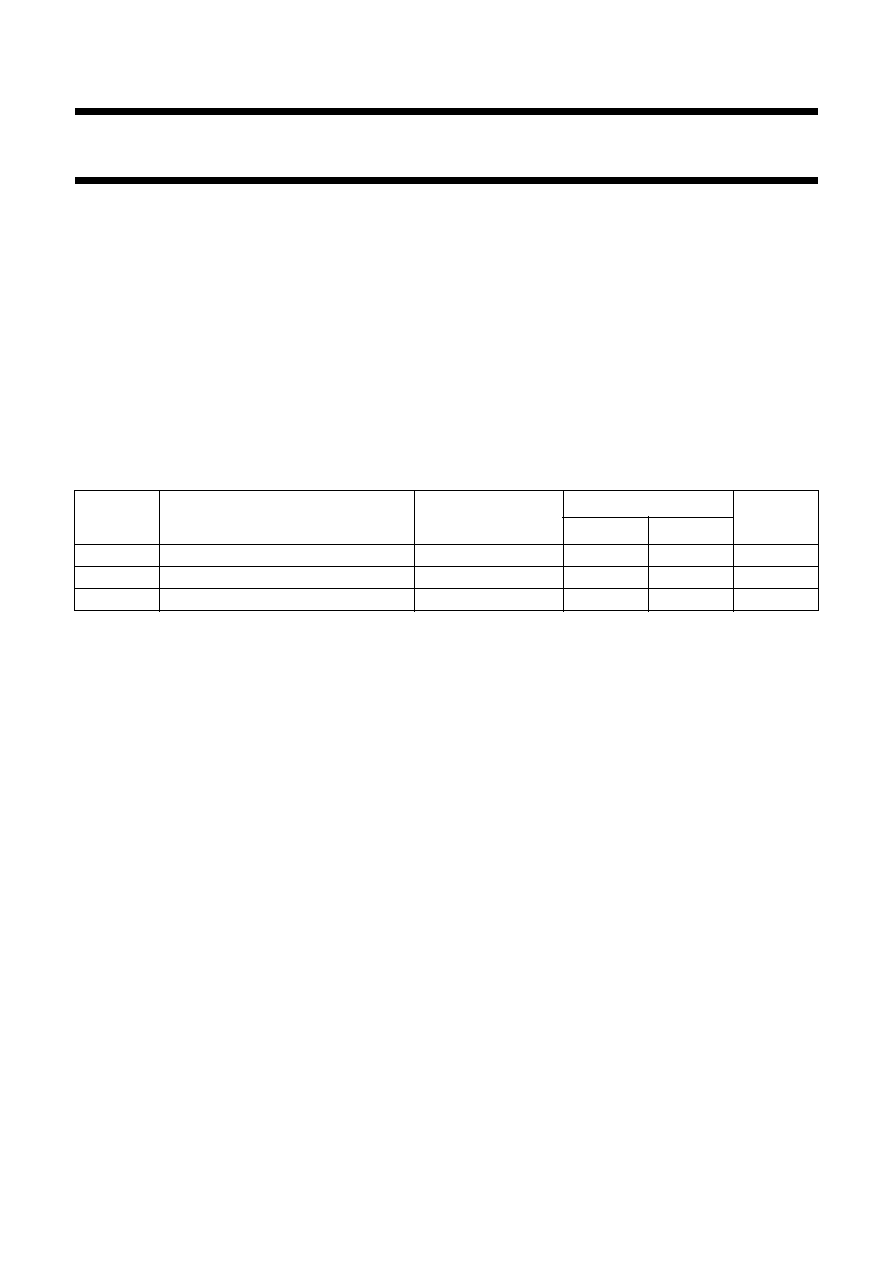
handbook, halfpage
1
14
GND
(1)
1A
VCC
7
2
3
4
5
6
1Y
2A
2Y
3A
3Y
13
12
11
10
9
6A
6Y
5A
5Y
4A
8
GND
Top view
4Y
MBL760
Fig.2 Pin configuration DHVQFN14.
(1) The die substrate is attached to this pad using conductive die
attach material. It can not be used as a supply pin or input.
handbook, halfpage
MNA840
1A
1Y
1
2
2A
2Y
3
4
3A
3Y
5
6
4A
4Y
9
8
5A
5Y
11
10
6A
6Y
13
12
Fig.3 Logic symbol.
handbook, halfpage
MNA841
2
1
4
3
6
5
8
9
10
11
12
13
Fig.4 IEC logic symbol.
2003 Oct 30
5
Philips Semiconductors
Product specification
Hex inverting Schmitt trigger
74HC14; 74HCT14
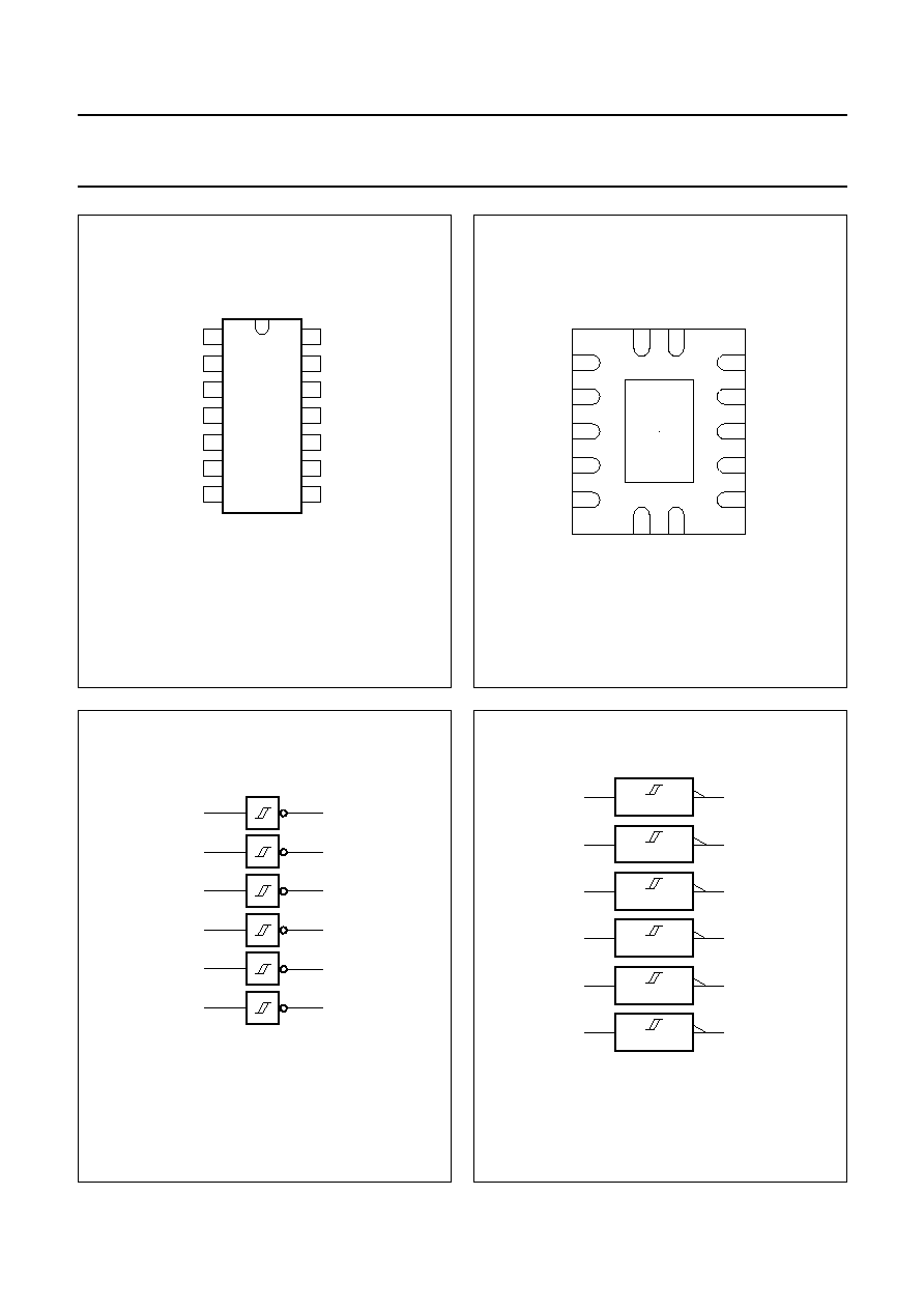
handbook, halfpage
MNA842
1A
1Y
1
2
2A
2Y
3
4
3A
3Y
5
6
4A
4Y
9
8
5A
5Y
11
10
6A
6Y
13
12
Fig.5 Functional diagram.
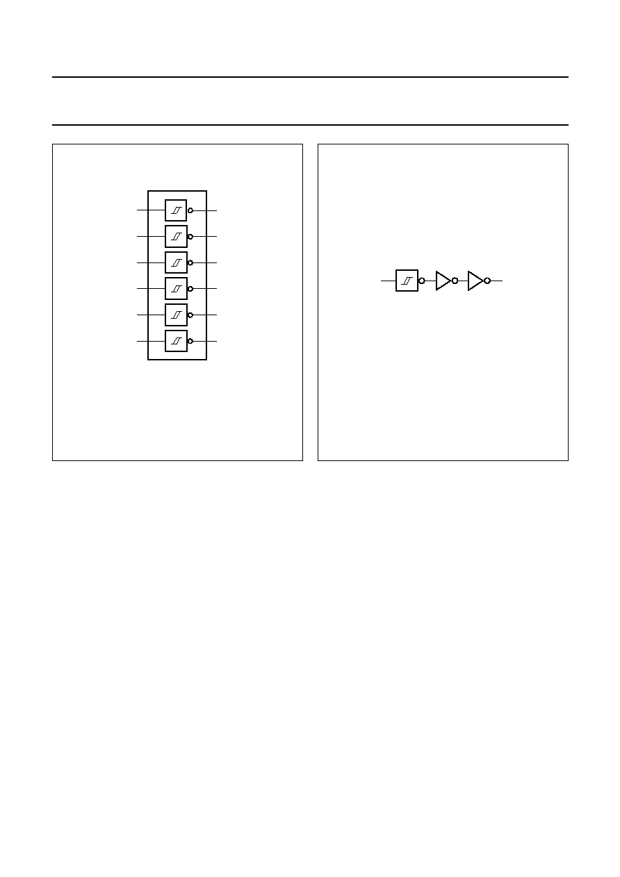
handbook, halfpage
MNA843
A
Y
Fig.6 Logic diagram (one Schmitt trigger).