Document Outline
- FEATURES
- DESCRIPTION
- QUICK REFERENCE DATA
- FUNCTION TABLE
- ORDERING INFORMATION
- PINNING
- RECOMMENDED OPERATING CONDITIONS
- LIMITING VALUES
- DC CHARACTERISTICS
- AC CHARACTERISTICS
- AC WAVEFORMS
- PACKAGE OUTLINES
- SOLDERING
- DATA SHEET STATUS
- DEFINITIONS
- DISCLAIMERS
DATA SHEET
Product specification
Supersedes data of 2001 Mar 02
2002 May 15
INTEGRATED CIRCUITS
74HC1G66; 74HCT1G66
Bilateral switch
2002 May 15
2
Philips Semiconductors
Product specification
Bilateral switch
74HC1G66; 74HCT1G66
FEATURES
∑
Wide operating voltage range from 2.0 to 9.0 V
∑
Very low ON-resistance:
≠ 45
(typical) at V
CC
= 4.5 V
≠ 30
(typical) at V
CC
= 6.0 V
≠ 25
(typical) at V
CC
= 9.0 V.
∑
High noise immunity
∑
Low power dissipation
∑
Very small 5 pins package
∑
Output capability: non standard.
DESCRIPTION
The 74HC1G/HCT1G66 is a high-speed Si-gate CMOS
device.
The 74HC1G/HCT1G66 provides an analog switch. The
switch has two input/output pins (Y and Z) and an active
HIGH enable input pin (E). When pin E is LOW, the analog
switch is turned off.
The non standard output currents are equal compared to
the 74HC/HCT4066.
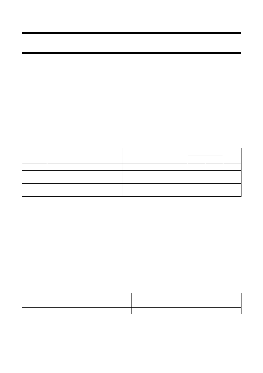
QUICK REFERENCE DATA
GND = 0 V; T
amb
= 25
∞
C; t
r
= t
f
= 6.0 ns.
Notes
1. C
PD
is used to determine the dynamic power dissipation (P
D
in
µ
W).
P
D
= C
PD
◊
V
CC
2
◊
f
i
+
((C
L
+C
S
)
◊
V
CC
2
◊
f
o
) where:
f
i
= input frequency in MHz;
f
o
= output frequency in MHz;
C
L
= output load capacitance in pF;
C
S
= maximum switch capacitance in pF;
V
CC
= supply voltage in Volts;
((C
L
+C
S
)
◊
V
CC
2
◊
f
o
) = sum of outputs.
2. For HC1G the condition is V
I
= GND to V
CC
.
For HCT1G the condition is V
I
= GND to V
CC
-
1.5 V.
FUNCTION TABLE
See note 1.
Note
1. H = HIGH voltage level;
L = LOW voltage level.
SYMBOL
PARAMETER
CONDITIONS
TYPICAL
UNIT
HC1G
HCT1G
t
PZH
/t
PZL
turn-on time E to V
os
C
L
= 15 pF; R
L
= 1 k
; V
CC
= 5 V 11
12
ns
t
PHZ
/t
PLZ
turn-off time E to V
os
C
L
= 15 pF; R
L
= 1 k
; V
CC
= 5 V 11
12
ns
C
I
input capacitance
1.5
1.5
pF
C
PD
power dissipation capacitance
notes 1 and 2
9
9
pF
C
S
maximum switch capacitance
8
8
pF
INPUT E
SWITCH
L
OFF
H
ON

2002 May 15
3
Philips Semiconductors
Product specification
Bilateral switch
74HC1G66; 74HCT1G66
ORDERING INFORMATION
PINNING
OUTSIDE NORTH
AMERICA
PACKAGE
TEMPERATURE
RANGE
PINS
PACKAGE
MATERIAL
CODE
MARKING
74HC1G66GW
-
40 to +125
∞
C
5
SC-88A
plastic
SOT353
HL
74HCT1G66GW
-
40 to +125
∞
C
5
SC-88A
plastic
SOT353
TL
74HC1G66GV
-
40 to +125
∞
C
5
SC-74A
plastic
SOT753
H66
74HCT1G66GV
-
40 to +125
∞
C
5
SC-74A
plastic
SOT753
T66
PIN
SYMBOL
DESCRIPTION
1
Y
independent input/output Y
2
Z
independent input/output Z
3
GND
ground (0 V)
4
E
enable input E (active HIGH)
5
V
CC
supply voltage
Fig.1 Pin configuration.
handbook, halfpage
1
2
3
5
4
MNA074
66
VCC
Z
E
GND
Y
Fig.2 Logic symbol.
handbook, halfpage
MNA075
4
1
2
Y
Z
E
Fig.3 IEC logic symbol.
handbook, halfpage
MNA076
4 #
1
2
X1
1
1
Fig.4 Logic diagram.
handbook, halfpage
MNA077
VCC
GND
E
Z
Y
VCC
2002 May 15
4
Philips Semiconductors
Product specification
Bilateral switch
74HC1G66; 74HCT1G66
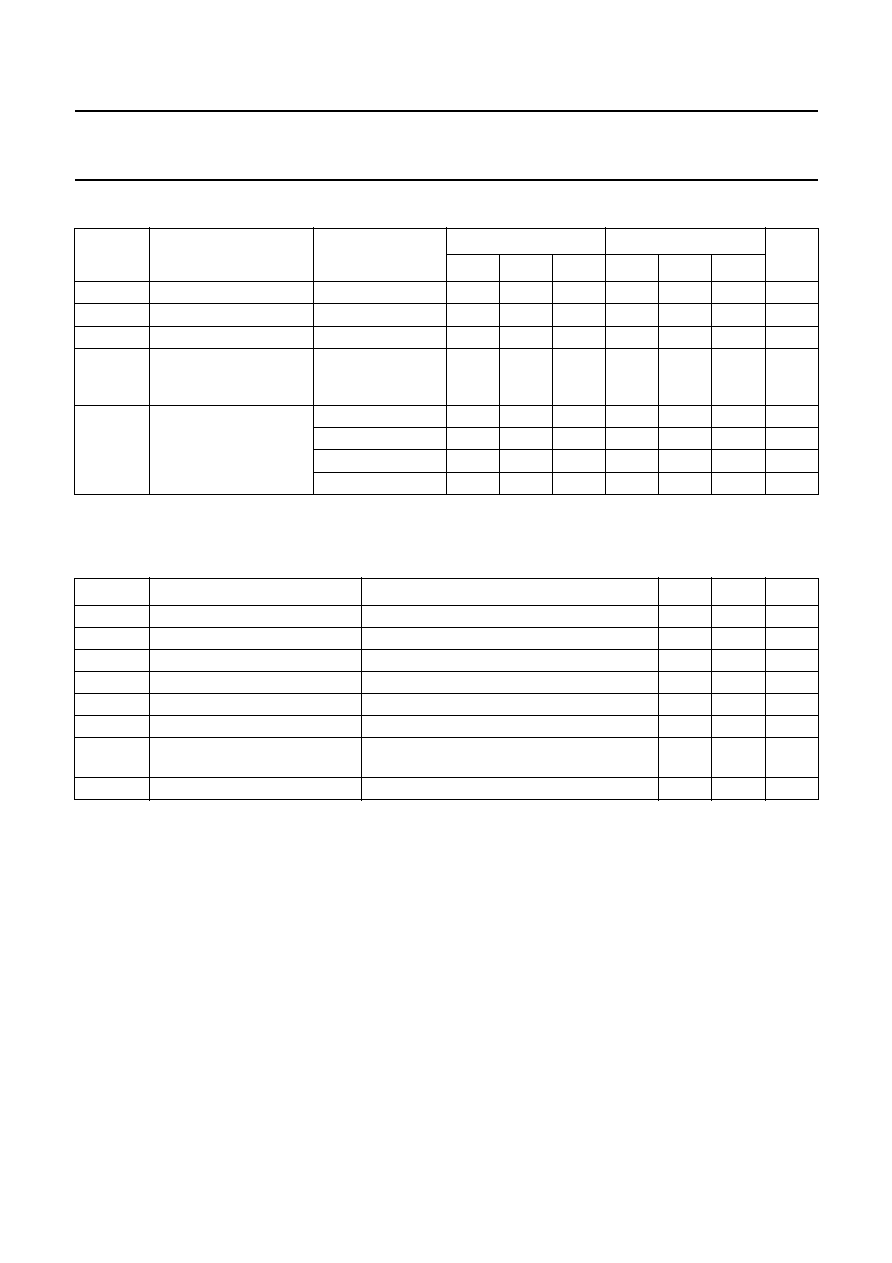
RECOMMENDED OPERATING CONDITIONS
LIMITING VALUES
In accordance with the Absolute Maximum Rating System (IEC 60134); voltages are referenced to GND (ground = 0 V);
see note 1.
Notes
1. To avoid drawing V
CC
current out of pin Z, when switch current flows in pin Y, the voltage drop across the
bidirectional switch must not exceed 0.4 V. If the switch current flows into pin Z, no V
CC
current will flow out of
terminal Y. In this case there is no limit for the voltage drop across the switch, but the voltage at pins Y and Z may
not exceed V
CC
or GND.
2. Above 55
∞
C the value of P
D
derates linearly with 2.5 mW/K.
SYMBOL
PARAMETER
CONDITIONS
74HC1G66
74HCT1G66
UNIT
MIN.
TYP.
MAX.
MIN.
TYP.
MAX.
V
CC
supply voltage
2.0
5.0
10.0
4.5
5.0
5.5
V
V
I
input voltage
GND
-
V
CC
GND
-
V
CC
V
V
S
switch voltage
GND
-
V
CC
GND
-
V
CC
V
T
amb
operating ambient
temperature
see DC and AC
characteristics per
device
-
40
-
+125
-
40
-
+125
∞
C
t
r
, t
f
input rise and fall times
V
CC
= 2.0 V
-
-
1000
-
-
-
ns
V
CC
= 4.5 V
-
6.0
500
-
6.0
500
ns
V
CC
= 6.0 V
-
-
400
-
-
-
ns
V
CC
= 10.0 V
-
-
250
-
-
-
ns
SYMBOL
PARAMETER
CONDITIONS
MIN.
MAX.
UNIT
V
CC
supply voltage
-
0.5
+11.0
V
I
IK
input diode current
V
I
< -
0.5 V or V
I
>
V
CC
+ 0.5 V
-
±
20
mA
I
SK
switch diode current
V
S
< -
0.5 V or V
S
>
V
CC
+ 0.5 V
-
±
20
mA
I
S
switch source or sink current
-
0.5 V
<
V
S
<
V
CC
+
0.5 V
-
±
25
mA
I
CC
V
CC
or GND current
-
±
50
mA
T
stg
storage temperature
-
65
+150
∞
C
P
D
power dissipation per package
for temperature range from
-
40 to
+
125
∞
C;
note 2
-
200
mW
P
S
power dissipation per switch
-
100
mW

2002 May 15
5
Philips Semiconductors
Product specification
Bilateral switch
74HC1G66; 74HCT1G66
DC CHARACTERISTICS
Family 74HC1G66
At recommended operating conditions; voltages are referenced to GND (ground = 0 V).
Note
1. All typical values are measured at T
amb
= 25
∞
C.
SYMBOL
PARAMETER
TEST CONDITIONS
T
amb
(
∞
C)
UNIT
OTHER
V
CC
(V)
-
40 to +85
-
40 to +125
MIN.
TYP.
(1)
MAX.
MIN.
MAX.
V
IH
HIGH-level input
voltage
2.0
1.5
1.2
-
1.5
-
V
4.5
3.15
2.4
-
3.15
-
V
6.0
4.2
3.2
-
4.2
-
V
9.0
6.3
4.7
-
6.3
-
V
V
IL
LOW-level input
voltage
2.0
-
0.8
0.5
-
0.5
V
4.5
-
2.1
1.35
-
1.35
V
6.0
-
2.8
1.8
-
1.8
V
9.0
-
4.3
2.7
-
2.7
V
I
LI
input leakage
current
V
I
= V
CC
or GND
6.0
-
0.1
1.0
-
1.0
µ
A
10.0
-
0.2
2.0
-
2.0
µ
A
I
S
analog switch
current, OFF-state
V
I
= V
IH
or V
IL
;
V
S
= V
CC
-
GND;
see Fig.6
10.0
-
0.1
1.0
-
1.0
µ
A
analog switch
current, ON-state
V
I
= V
IH
or V
IL
;
V
S
= V
CC
-
GND;
see Fig.7
10.0
-
0.1
1.0
-
1.0
µ
A
I
CC
quiescent supply
current
V
I
= V
CC
or GND;
V
is
= GND or V
CC
;
V
os
= V
CC
or GND
6.0
-
1.0
10
-
20
µ
A
10.0
-
2.0
20
-
40
µ
A