2004 May 19
2
Philips Semiconductors
Product specification
Bilateral switches
74HC2G66; 74HCT2G66
FEATURES
·
Wide supply voltage range from 2.0 V to 9.0 V
·
Very low ON-resistance:
41
(typical) at V
CC
= 4.5 V
30
(typical) at V
CC
= 6.0 V
21
(typical) at V
CC
= 9.0 V.
·
High noise immunity
·
Low power dissipation
· ±
25 mA switch current
·
SOT505-2 package
·
ESD protection:
HBM EIA/JESD22-A114-A exceeds 2000 V
MM EIA/JESD22-A115-A exceeds 200 V.
·
Specified from
-
40
°
C to +85
°
C and
-
40
°
C to +125
°
C.
DESCRIPTION
The 74HC2G66/74HCT2G66 is a high-speed Si-gate
CMOS device.
The 74HC2G66/74HCT2G66 provides a dual analog
switch. Each switch has two pins (nY and nZ) for input or
output and an active HIGH enable input (pin E). When
pin E is LOW, the belonging analog switch is turned off.
QUICK REFERENCE DATA
GND = 0 V; T
amb
= 25
°
C; t
r
= t
f
= 6.0 ns; V
os
is the output voltage at pins nY or nZ, whichever is assigned as an output.
Notes
1. C
PD
is used to determine the dynamic power dissipation (P
D
in
µ
W).
P
D
= C
PD
×
V
CC
2
×
f
i
+ (C
L
+C
S
)
×
V
CC
2
×
f
o
) where:
f
i
= input frequency in MHz;
f
o
= output frequency in MHz;
C
L
= output load capacitance in pF;
C
S
= Switch capacitance in pF;
V
CC
= supply voltage in Volts.
2. For 74HC2G66 the condition is V
I
= GND to V
CC
.
For 74HCT2G66 the condition is V
I
= GND to V
CC
-
1.5 V.
SYMBOL
PARAMETER
CONDITIONS
TYPICAL
UNIT
HC2G
HCT2G
t
PZH
/t
PZL
turn-on time nE to V
os
C
L
= 50 pF; R
L
= 1 k
; V
CC
= 4.5 V 12
13
ns
t
PHZ
/t
PLZ
turn-off time nE to V
os
C
L
= 50 pF; R
L
= 1 k
; V
CC
= 4.5 V 12
13
ns
C
I
input capacitance
3.5
3.5
pF
C
PD
power dissipation capacitance per switch notes 1 and 2
9
9
pF
C
S
switch capacitance
8
8
pF

2004 May 19
3
Philips Semiconductors
Product specification
Bilateral switches
74HC2G66; 74HCT2G66
FUNCTION TABLE
See note 1.
Note
1. H = HIGH voltage level;
L = LOW voltage level.
ORDERING INFORMATION
PINNING
INPUT nE
SWITCH
L
OFF
H
ON
TYPE NUMBER
PACKAGE
TEMPERATURE
RANGE
PINS
PACKAGE
MATERIAL
OUTLINE
VERSION
MARKING
74HC2G66DP
-
40
°
C to +125
°
C
8
TSSOP8
plastic
SOT505-2
H66
74HCT2G66DP
-
40
°
C to +125
°
C
8
TSSOP8
plastic
SOT505-2
T66
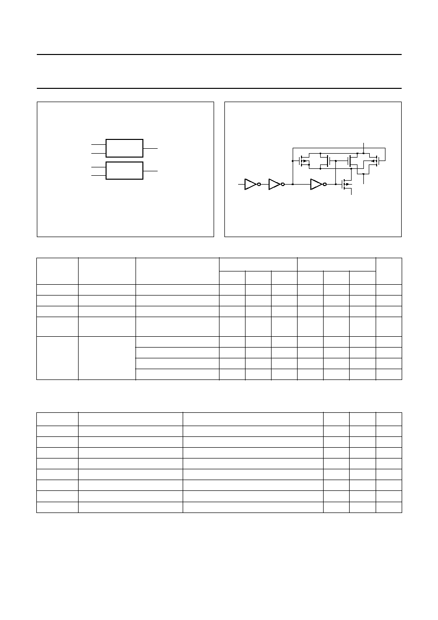
PIN
SYMBOL
DESCRIPTION
1
1Y
independent input or output
2
1Z
independent input or output
3
2E
enable input (active HIGH)
4
GND
ground (0 V)
5
2Y
independent input or output
6
2Z
independent input or output
7
1E
enable input (active HIGH)
8
V
CC
supply voltage
handbook, halfpage
66
MNB002
1
2
3
4
1Y
1Z
2E
GND
VCC
1E
2Z
2Y
8
7
6
5
Fig.1 Pin configuration.
MNB003
handbook, halfpage
1Y
1E
2Z
1Z
2Y
2E
Fig.2 Logic symbol.
2004 May 19
4
Philips Semiconductors
Product specification
Bilateral switches
74HC2G66; 74HCT2G66
MNB004
handbook, halfpage
2
1
1
1
1
X1
6
5
7 #
1
X1
#
3
Fig.3 IEC logic symbol.
handbook, halfpage
MNB005
GND
nZ
nY
nE
Fig.4 Logic diagram.
RECOMMENDED OPERATING CONDITIONS
LIMITING VALUES
In accordance with the Absolute Maximum Rating System (IEC 60134); voltages are referenced to GND (ground = 0 V).
Notes
1. The input and output voltage ratings may be exceeded if the input and output current ratings are observed.
2. Above 55
°
C the value of P
tot
derates linearly with 2.5 mW/K.
SYMBOL
PARAMETER
CONDITIONS
74HC2G66
74HCT2G66
UNIT
MIN.
TYP.
MAX.
MIN.
TYP.
MAX.
V
CC
supply voltage
2.0
5.0
10.0
4.5
5.0
5.5
V
V
I
input voltage
0
-
V
CC
0
-
V
CC
V
V
O
output voltage
0
-
V
CC
0
-
V
CC
V
T
amb
ambient
temperature
see DC and AC
characteristics per device
-
40
+25
+125
-
40
+25
+125
°
C
t
r
, t
f
input rise and fall
times
V
CC
= 2.0 V
-
-
1000
-
-
-
ns
V
CC
= 4.5 V
-
6.0
500
-
6.0
500
ns
V
CC
= 6.0 V
-
-
400
-
-
-
ns
V
CC
= 9.0 V
-
-
250
-
-
-
ns
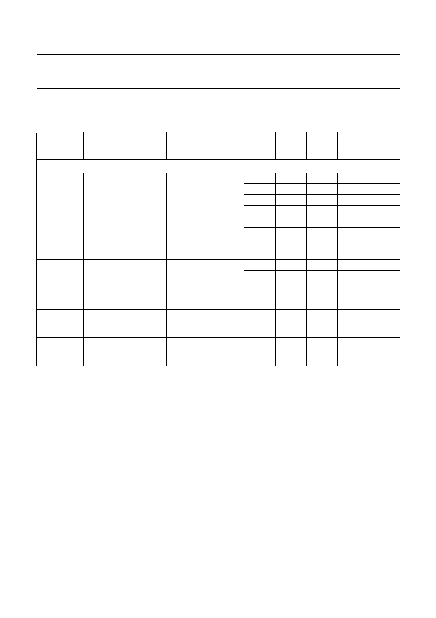
SYMBOL
PARAMETER
CONDITIONS
MIN.
MAX.
UNIT
V
CC
supply voltage
-
0.5
+11.0
V
I
IK
input diode current
V
I
<
-
0.5 V or V
I
> V
CC
+ 0.5 V; note 1
-
±
20
mA
I
OK
output diode current
V
O
<
-
0.5 V or V
O
> V
CC
+ 0.5 V; note 1
-
±
20
mA
I
O
output source or sink current
-
0.5 V < V
O
< V
CC
+ 0.5 V; note 1
-
±
25
mA
I
CC
, I
GND
V
CC
or GND current
note 1
-
±
30
mA
T
stg
storage temperature
-
65
+150
°
C
P
tot
power dissipation of package
T
amb
=
-
40
°
C to +125
°
C; note 2
-
300
mW
P
s
power dissipation per switch
-
100
mW
2004 May 19
5
Philips Semiconductors
Product specification
Bilateral switches
74HC2G66; 74HCT2G66
DC CHARACTERISTICS
Type 74HC2G66
At recommended operating conditions; voltages are referenced to GND (ground = 0 V).
SYMBOL
PARAMETER
TEST CONDITIONS
MIN.
TYP.
MAX.
UNIT
OTHER
V
CC
(V)
T
amb
=
-
40
°
C to +85
°
C; note1
V
IH
HIGH-level input voltage
2.0
1.5
1.2
-
V
4.5
3.15
2.4
-
V
6.0
4.2
3.2
-
V
9.0
6.3
4.7
-
V
V
IL
LOW-level input voltage
2.0
-
0.8
0.5
V
4.5
-
2.1
1.35
V
6.0
-
2.8
1.8
V
9.0
-
4.3
2.7
V
I
LI
input leakage current
V
I
= V
CC
or GND
6.0
-
-
±
0.1
µ
A
9.0
-
-
±
0.2
µ
A
I
s(OFF)
analog switch current,
OFF-state
V
I
= V
IH
or V
IL
;
V
S
= V
CC
-
GND;
see Fig.7
9.0
-
0.1
1.0
µ
A
I
s(ON)
analog switch current,
ON-state
V
I
= V
IH
or V
IL
;
V
S
= V
CC
-
GND;
see Fig.8
9.0
-
0.1
1.0
µ
A
I
CC
quiescent supply current
V
I
= V
CC
or GND;
V
is
= GND or V
CC
;
V
os
= V
CC
or GND
6.0
-
-
10
µ
A
9.0
-
-
20
µ
A