DATA SHEET
Product specification
File under Integrated Circuits, IC06
December 1990
INTEGRATED CIRCUITS
74HC/HCT4094
8-stage shift-and-store bus register
For a complete data sheet, please also download:
∑
The IC06 74HC/HCT/HCU/HCMOS Logic Family Specifications
∑
The IC06 74HC/HCT/HCU/HCMOS Logic Package Information
∑
The IC06 74HC/HCT/HCU/HCMOS Logic Package Outlines
December 1990
2
Philips Semiconductors
Product specification
8-stage shift-and-store bus register
74HC/HCT4094
FEATURES
∑
Output capability: standard
∑
I
CC
category: MSI
GENERAL DESCRIPTION
The 74HC/HCT4094 are high-speed Si-gate CMOS
devices and are pin compatible with the "4094" of the
"4000B" series. They are specified in compliance with
JEDEC standard no. 7A.
The 74HC/HCT4094 are 8-stage serial shift registers
having a storage latch associated with each stage for
strobing data from the serial input (D) to the parallel
buffered 3-state outputs (QP
0
to QP
7
). The parallel outputs
may be connected directly to common bus lines.
Data is shifted on the positive-going clock (CP) transitions.
The data in each shift register stage is transferred to the
storage register when the strobe input (STR) is HIGH.
Data in the storage register appears at the outputs
whenever the output enable input (OE) signal is HIGH.
Two serial outputs (QS
1
and QS
2
) are available for
cascading a number of "4094" devices. Data is available at
QS
1
on the positive-going clock edges to allow high-speed
operation in cascaded systems in which the clock rise time
is fast. The same serial information is available at QS
2
on
the next negative-going clock edge and is for cascading
"4094" devices when the clock rise time is slow.
APPLICATIONS
∑
Serial-to-parallel data conversion
∑
Remote control holding register
QUICK REFERENCE DATA
GND = 0 V; T
amb
= 25
∞
C; t
r
= t
f
= 6 ns
Notes
1. C
PD
is used to determine the dynamic power dissipation (P
D
in
µ
W):
P
D
= C
PD
◊
V
CC
2
◊
f
i
+
(C
L
◊
V
CC
2
◊
f
o
) where:
f
i
= input frequency in MHz
f
o
= output frequency in MHz
(C
L
◊
V
CC
2
◊
f
o
) = sum of outputs
C
L
= output load capacitance in pF
V
CC
= supply voltage in V
2. For HC the condition is V
I
= GND to V
CC
For HCT the condition is V
I
= GND to V
CC
-
1.5 V
ORDERING INFORMATION
See
"74HC/HCT/HCU/HCMOS Logic Package Information"
.
SYMBOL
PARAMETER
CONDITIONS
TYPICAL
UNIT
HC
HCT
t
PHL
/ t
PLH
propagation delay
C
L
= 15 pF; V
CC
= 5 V
CP to QS
1
15
19
ns
CP to QS
2
13
18
ns
CP to QP
n
20
21
ns
STR to QP
n
18
19
ns
f
max
maximum clock frequency
95
86
MHz
C
I
input capacitance
3.5
3.5
pF
C
PD
power dissipation capacitance per package
notes 1 and 2
83
92
pF
December 1990
3
Philips Semiconductors
Product specification
8-stage shift-and-store bus register
74HC/HCT4094
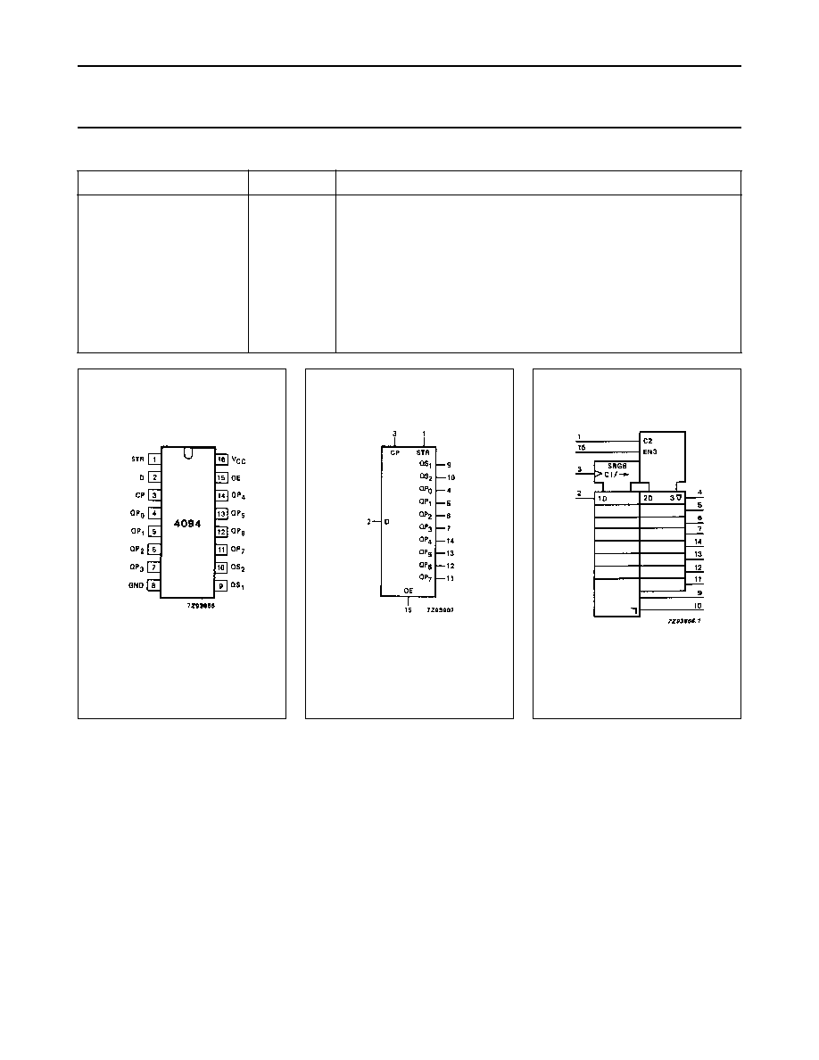
PIN DESCRIPTION
PIN NO.
SYMBOL
NAME AND FUNCTION
1
STR
strobe input
2
D
serial input
3
CP
clock input
4, 5, 6, 7,14, 13, 12, 11
QP
0
to QP
7
parallel outputs
8
GND
ground (0 V)
9, 10
QS
1
, QS
2
serial outputs
15
OE
output enable input
16
V
CC
positive supply voltage
Fig.1 Pin configuration.
Fig.2 Logic symbol.
Fig.3 IEC logic symbol.
December 1990
4
Philips Semiconductors
Product specification
8-stage shift-and-store bus register
74HC/HCT4094
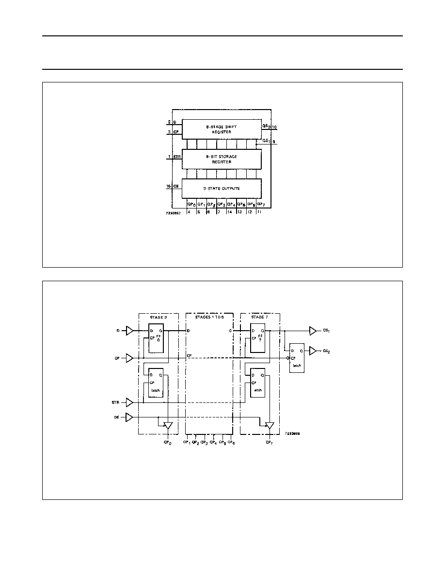
Fig.4 Functional diagram.
Fig.5 Logic diagram.
December 1990
5
Philips Semiconductors
Product specification
8-stage shift-and-store bus register
74HC/HCT4094
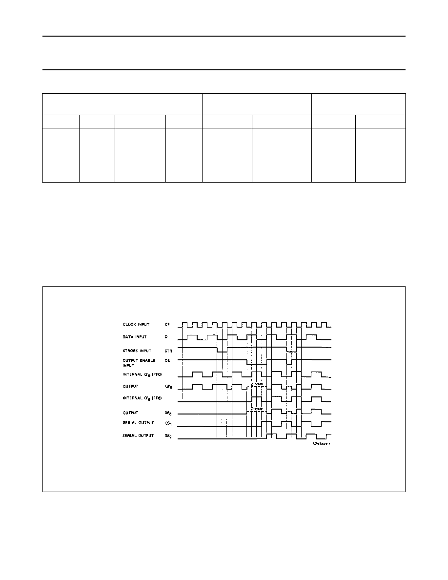
FUNCTION TABLE
Notes
1. H = HIGH voltage level
L = LOW voltage level
X = don't care
Z = high impedance OFF-state
NC= no change
= LOW-to-HIGH CP transition
= HIGH-to-LOW CP transition
Q'
6
= the information in the seventh register stage is transferred to the 8th register stage and QS
n
output at the
positive clock edge
INPUTS
PARALLEL OUTPUTS
SERIAL
OUTPUTS
CP
OE
STR
D
QP
0
QP
n
QS
1
QS
2
L
L
H
H
H
H
X
X
L
H
H
H
X
X
X
L
H
H
Z
Z
NC
L
H
NC
Z
Z
NC
QP
n - 1
QP
n - 1
NC
Q'
6
NC
Q'
6
Q'
6
Q'
6
NC
NC
QP
7
NC
NC
NC
QP
7
Fig.6 Timing diagram.
December 1990
6
Philips Semiconductors
Product specification
8-stage shift-and-store bus register
74HC/HCT4094
DC CHARACTERISTICS FOR 74HC
For the DC characteristics see
"74HC/HCT/HCU/HCMOS Logic Family Specifications"
.
Output capability: standard
I
CC
category: MSI
AC CHARACTERISTICS FOR 74HC
GND = 0 V; t
r
= t
f
= 6 ns; C
L
= 50 pF
SYMBOL PARAMETER
T
amb
(
∞
C)
UNIT
TEST CONDITIONS
74HC
V
CC
(V)
WAVEFORMS
+
25
-
40 to
+
85
-
40 to
+
125
min. typ. max. min. max. min.
max.
t
PHL
/ t
PLH
propagation delay
CP to QS
1
50
18
14
150
30
26
190
38
33
225
45
38
ns
2.0
4.5
6.0
Fig.7
t
PHL
/ t
PLH
propagation delay
CP to QS
2
44
16
13
135
27
23
170
34
29
205
41
35
ns
2.0
4.5
6.0
Fig.7
t
PHL
/ t
PLH
propagation delay
CP to QP
n
63
23
18
195
39
33
245
49
42
295
59
50
ns
2.0
4.5
6.0
Fig.7
t
PHL
/ t
PLH
propagation delay
STR to QP
n
58
21
17
180
36
31
225
45
38
270
54
46
ns
2.0
4.5
6.0
Fig.8
t
PZH
/ t
PZL
3-state output enable time
OE to QP
n
55
20
16
175
35
30
220
44
37
265
53
45
ns
2.0
4.5
6.0
Fig.9
t
PHZ
/ t
PLZ
3-state output disable
time OE to QP
n
41
15
12
125
25
21
155
31
26
190
38
32
ns
2.0
4.5
6.0
Fig.9
t
THL
/ t
TLH
output transition time
19
7
6
75
15
13
95
19
16
110
22
19
ns
2.0
4.5
Fig.7
t
W
clock pulse width
HIGH or LOW
80
16
14
14
5
4
100
20
17
120
24
20
ns
2.0
4.5
6.0
Fig.7
t
W
strobe pulse width
HIGH
80
16
14
14
5
4
100
20
17
120
24
20
ns
2.0
4.5
6.0
Fig.8
t
su
set-up time
D to CP
50
10
9
14
5
4
65
13
11
75
15
13
ns
2.0
4.5
6.0
Fig.10
t
su
set-up time
CP to STR
100
20
17
28
10
8
125
25
21
150
30
26
ns
2.0
4.5
6.0
Fig.8
December 1990
7
Philips Semiconductors
Product specification
8-stage shift-and-store bus register
74HC/HCT4094
t
h
hold time
D to CP
3
3
3
-
6
-
2
-
2
3
3
3
3
3
3
ns
2.0
4.5
6.0
Fig.10
t
h
hold time
CP to STR
0
0
0
-
14
-
5
-
4
0
0
0
0
0
0
ns
2.0
4.5
6.0
Fig.8
f
max
maximum clock pulse
frequency
6.0
30
35
28
87
103
4.8
24
28
4.0
20
24
MHz
2.0
4.5
6.0
Fig.7
SYMBOL PARAMETER
T
amb
(
∞
C)
UNIT
TEST CONDITIONS
74HC
V
CC
(V)
WAVEFORMS
+
25
-
40 to
+
85
-
40 to
+
125
min. typ. max. min. max. min.
max.

December 1990
8
Philips Semiconductors
Product specification
8-stage shift-and-store bus register
74HC/HCT4094
DC CHARACTERISTICS FOR 74HCT
For the DC characteristics see
"74HC/HCT/HCU/HCMOS Logic Family Specifications"
.
Output capability: standard
I
CC
category: MSI
Note to HCT types
The value of additional quiescent supply current (
I
CC
) for a unit load of 1 is given in the family specifications.
To determine
I
CC
per input, multiply this value by the unit load coefficient shown in the table below.
INPUT
UNIT LOAD COEFFICIENT
OE, CP
D
STR
1.50
0.40
1.00

December 1990
9
Philips Semiconductors
Product specification
8-stage shift-and-store bus register
74HC/HCT4094
AC CHARACTERISTICS FOR 74HCT
GND = 0 V; t
r
= t
f
= 6 ns; C
L
= 50 pF
SYMBOL PARAMETER
T
amb
(
∞
C)
UNIT
TEST CONDITIONS
74HCT
V
CC
(V)
WAVEFORMS
+
25
-
40 to
+
85
-
40 to
+
125
min. typ. max. min. max. min.
max.
t
PHL
/ t
PLH
propagation delay
CP to QS
1
23
39
49
59
ns
4.5
Fig.7
t
PHL
/ t
PLH
propagation delay
CP to QS
2
21
36
45
54
ns
4.5
Fig.7
t
PHL
/ t
PLH
propagation delay
CP to QP
n
25
43
54
65
ns
4.5
Fig.7
t
PHL
/ t
PLH
propagation delay
STR to QP
n
22
39
49
59
ns
4.5
Fig.8
t
PZH
/ t
PZL
3-state output enable time
OE to QP
n
20
35
44
53
ns
4.5
Fig.9
t
PHZ
/ t
PLZ
3-state output disable time
OE to QP
n
21
35
44
53
ns
4.5
Fig.9
t
THL
/ t
TLH
output transition time
7
15
19
22
ns
4.5
Fig.7
t
W
clock pulse width
HIGH or LOW
16
7
20
24
ns
4.5
Fig.7
t
W
strobe pulse width
HIGH
16
5
20
24
ns
4.5
Fig.8
t
su
set-up time
D to CP
10
4
13
15
ns
4.5
Fig.10
t
su
set-up time
CP to STR
20
9
25
30
ns
4.5
Fig.8
t
h
hold time
D to CP
4
0
4
4
ns
4.5
Fig.10
t
h
hold time
CP to STR
0
-
4
0
0
ns
4.5
Fig.8
f
max
maximum clock pulse
frequency
30
80
24
20
MHz
4.5
Fig.7
December 1990
10
Philips Semiconductors
Product specification
8-stage shift-and-store bus register
74HC/HCT4094
AC WAVEFORMS
Fig.7
Waveforms showing the clock (CP) to
output (QP
n
, QS
1
, QS
2
) propagation
delays, the clock pulse width and the
maximum clock frequency.
(1) HC : V
M
= 50%; V
I
= GND to V
CC
.
HCT: V
M
= 1.3 V; V
I
= GND to 3 V.
Fig.8
Waveforms showing the strobe (STR) to
output (QP
n
) propagation delays and the
strobe pulse width and the clock set-up and
hold times for the strobe input.
(1) HC : V
M
= 50%; V
I
= GND to V
CC
.
HCT: V
M
= 1.3 V; V
I
= GND to 3 V.
Fig.9
Waveforms showing the 3-state enable and
disable times for input OE.
(1) HC : V
M
= 50%; V
I
= GND to V
CC
.
HCT: V
M
= 1.3 V; V
I
= GND to 3 V.
PACKAGE OUTLINES
See
"74HC/HCT/HCU/HCMOS Logic Package Outlines"
.
Fig.10 Waveforms showing the data set-up and
hold times for the data input (D).
The shaded areas indicate when the input is
permitted to change for predictable output
performance.
(1) HC : V
M
= 50%; V
I
= GND to V
CC
.
HCT: V
M
= 1.3 V; V
I
= GND to 3 V.