 | –≠–ª–µ–∫—Ç—Ä–æ–Ω–Ω—ã–π –∫–æ–º–ø–æ–Ω–µ–Ω—Ç: 74HCT4316 | –°–∫–∞—á–∞—Ç—å:  PDF PDF  ZIP ZIP |
DATA SHEET
Product specification
File under Integrated Circuits, IC06
September 1993
INTEGRATED CIRCUITS
74HC/HCT4316
Quad bilateral switches
For a complete data sheet, please also download:
∑
The IC06 74HC/HCT/HCU/HCMOS Logic Family Specifications
∑
The IC06 74HC/HCT/HCU/HCMOS Logic Package Information
∑
The IC06 74HC/HCT/HCU/HCMOS Logic Package Outlines
September 1993
2
Philips Semiconductors
Product specification
Quad bilateral switches
74HC/HCT4316
FEATURES
∑
Low "ON" resistance:
160
(typ.) at V
CC
-
V
EE
= 4.5 V
120
(typ.) at V
CC
-
V
EE
= 6.0 V
80
(typ.) at V
CC
-
V
EE
= 9.0 V
∑
Logic level translation:
to enable 5 V logic to communicate
with
±
5 V analog signals
∑
Typical "break before make" built in
∑
Output capability: non-standard
∑
I
CC
category: MSI
GENERAL DESCRIPTION
The 74HC/HCT4316 are high-speed Si-gate CMOS
devices. They are specified in compliance with JEDEC
standard no. 7A.
The 74HC/HCT4316 have four independent analog
switches. Each switch has two input/output terminals
(nY, nZ) and an active HIGH select input (nS). When the
enable input (E) is HIGH, all four analog switches are
turned off.
Current through a switch will not cause additional V
CC
current provided the voltage at the terminals of the switch
is maintained within the supply voltage range;
V
CC
>>
(V
Y
, V
Z
)
>>
V
EE
. Inputs nY and nZ are electrically
equivalent terminals.
V
CC
and GND are the supply voltage pins for the digital
control inputs (E and nS). The V
CC
to GND ranges are 2.0
to 10.0 V for HC and 4.5 to 5.5 V for HCT.
The analog inputs/outputs (nY and nZ) can swing between
V
CC
as a positive limit and V
EE
as a negative limit.
V
CC
-
V
EE
may not exceed 10.0 V.
See the "4016" for the version without logic level
translation.
QUICK REFERENCE DATA
V
EE
= GND = 0 V; T
amb
= 25
∞
C; t
r
= t
f
= 6 ns
SYMBOL
PARAMETER
CONDITIONS
TYPICAL
UNIT
HC
HCT
t
PZH
turn "ON" time
C
L
= 15 pF; R
L
= 1 k
;
V
CC
= 5 V
E to V
OS
19
19
ns
nS to V
OS
16
17
ns
t
PZL
turn "ON" time
E to V
OS
19
24
ns
nS to V
OS
16
21
ns
t
PHZ
/ t
PLZ
turn "OFF" time
E to V
OS
20
21
ns
nS to V
OS
16
19
ns
C
I
input capacitance
3.5
3.5
pF
C
PD
power dissipation capacitance per switch
notes 1 and 2
13
14
pF
C
S
max. switch capacitance
5
5
pF
Notes
1. C
PD
is used to determine the dynamic power
dissipation (P
D
in
µ
W):
P
D
= C
PD
◊
V
CC
2
◊
f
i
+
{ (C
L
+
C
S
)
◊
V
CC
2
◊
f
o
}
where:
f
i
= input frequency in MHz
f
o
= output frequency in MHz
{ (C
L
+
C
S
)
◊
V
CC
2
◊
f
o
} = sum of outputs
C
L
= output load capacitance in pF
C
S
= max. switch capacitance in pF
V
CC
= supply voltage in V
2. For HC the condition is V
I
= GND to V
CC
For HCT the condition is V
I
= GND to V
CC
-
1.5 V
September 1993
3
Philips Semiconductors
Product specification
Quad bilateral switches
74HC/HCT4316
ORDERING INFORMATION
See
"74HC/HCT/HCU/HCMOS Logic Package Information"
.
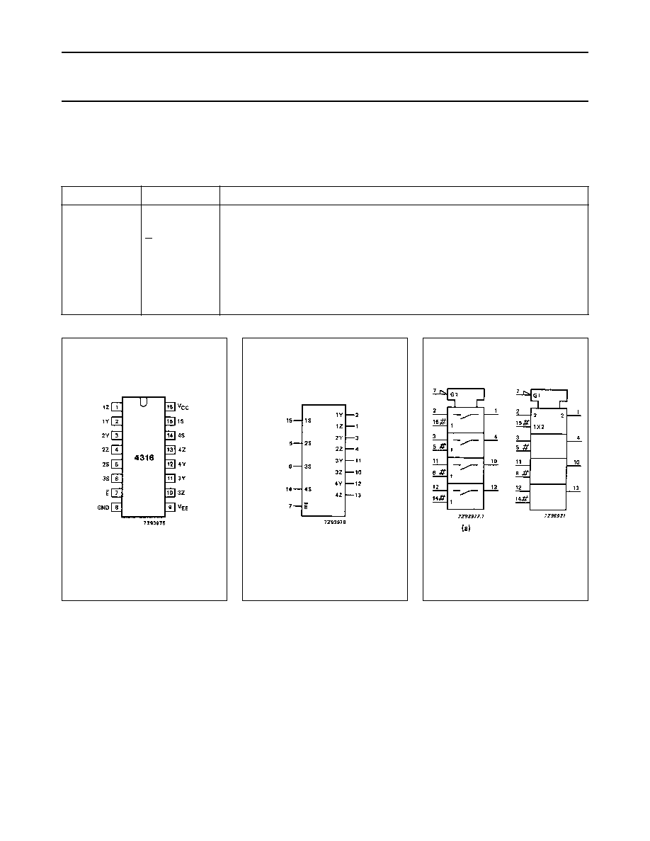
PIN DESCRIPTION
PIN NO.
SYMBOL
NAME AND FUNCTION
1, 4, 10, 13
1Z to 4Z
independent inputs/outputs
2, 3, 11, 12
1Y to 4Y
independent inputs/outputs
7
E
enable input (active LOW)
8
GND
ground (0 V)
9
V
EE
negative supply voltage
15, 5, 6, 14
1S to 4S
select inputs (active HIGH)
16
V
CC
positive supply voltage
Fig.1 Pin configuration.
Fig.2 Logic symbol.
Fig.3 IEC logic symbol.
(b)

September 1993
4
Philips Semiconductors
Product specification
Quad bilateral switches
74HC/HCT4316
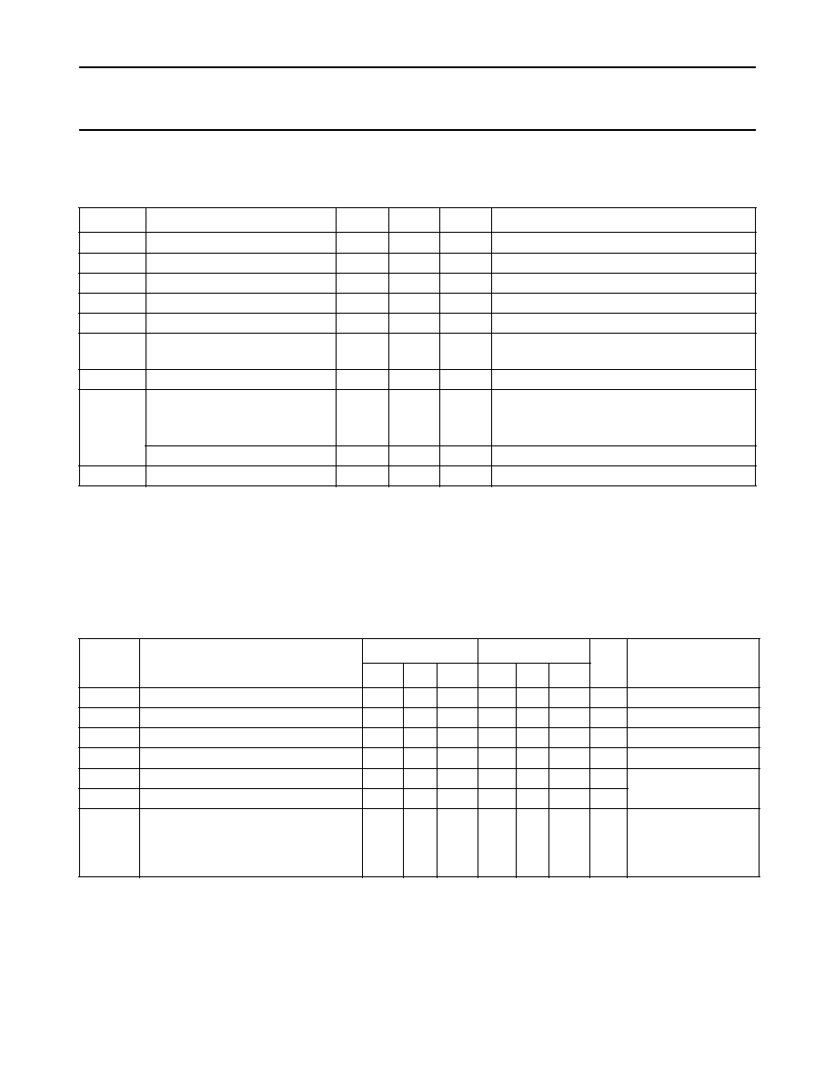
FUNCTION TABLE
Note
1. H = HIGH voltage level
L = LOW voltage level
X = don't care
APPLICATIONS
∑
Signal gating
∑
Modulation
∑
Demodulation
∑
Chopper
INPUTS
SWITCH
E
nS
L
L
L
H
off
on
H
X
off
Fig.4 Functional diagram.
Fig.5 Schematic diagram (one switch).
September 1993
5
Philips Semiconductors
Product specification
Quad bilateral switches
74HC/HCT4316
RATINGS
Limiting values in accordance with the Absolute Maximum System (IEC 134)
Voltages are referenced to V
EE
= GND (ground = 0 V)
Note to ratings
To avoid drawing V
CC
current out of terminal Z, when switch current flows in terminals Y
n
, the voltage drop across the
bidirectional switch must not exceed 0.4 V. If the switch current flows into terminals Z, no V
CC
current will flow out of
terminal Y
n
. In this case there is no limit for the voltage drop across the switch, but the voltages at Y
n
and Z may not
exceed V
CC
or V
EE
.
RECOMMENDED OPERATING CONDITIONS
SYMBOL
PARAMETER
MIN.
MAX.
UNIT
CONDITIONS
V
CC
DC supply voltage
-
0.5
+
11.0
V
±
I
IK
DC digital input diode current
20
mA
for V
I
< -
0.5 V or V
I
>
V
CC
+
0.5 V
±
I
SK
DC switch diode current
20
mA
for V
S
< -
0.5 V or V
S
>
V
CC
+
0.5 V
±
I
S
DC switch current
25
mA
for
-
0.5 V
<
V
S
<
V
CC
+
0.5 V
±
I
EE
DC V
EE
current
20
mA
±
I
CC
;
±
I
GND
DC V
CC
or GND current
50
mA
T
stg
storage temperature range
-
65
+
150
∞
C
P
tot
power dissipation per package
for temperature range:
-
40 to
+
125
∞
C
74HC/HCT
plastic DIL
750
mW
above
+
70
∞
C: derate linearly with 12 mW/K
plastic mini-pack (SO)
500
mW
above
+
70
∞
C: derate linearly with 8 mW/K
P
S
power dissipation per switch
100
mW
SYMBOL
PARAMETER
74HC
74HCT
UNIT
CONDITIONS
min.
typ. max. min. typ. max.
V
CC
DC supply voltage V
CC
-
GND
2.0
5.0
10.0
4.5
5.0
5.5
V
see Figs 6 and 7
V
CC
DC supply voltage V
CC
-
V
EE
2.0
5.0
10.0
2.0
5.0
10.0
V
see Figs 6 and 7
V
I
DC input voltage range
GND
V
CC
GND
V
CC
V
V
S
DC switch voltage range
V
EE
V
CC
V
EE
V
CC
V
T
amb
operating ambient temperature range
-
40
+
85
-
40
+
85
∞
C
see DC and AC
CHARACTERISTICS
T
amb
operating ambient temperature range
-
40
+
125
-
40
+
125
∞
C
t
r
, t
f
input rise and fall times
6.0
1000
500
400
250
6.0
500
ns
V
CC
= 2.0 V
V
CC
= 4.5 V
V
CC
= 6.0 V
V
CC
= 10.0 V