DATA SHEET
Product specification
File under Integrated Circuits, IC06
December 1990
INTEGRATED CIRCUITS
74HC/HCT4510
BCD up/down counter
For a complete data sheet, please also download:
∑
The IC06 74HC/HCT/HCU/HCMOS Logic Family Specifications
∑
The IC06 74HC/HCT/HCU/HCMOS Logic Package Information
∑
The IC06 74HC/HCT/HCU/HCMOS Logic Package Outlines
December 1990
2
Philips Semiconductors
Product specification
BCD up/down counter
74HC/HCT4510
FEATURES
∑
Output capability: standard
∑
I
CC
category: MSI
GENERAL DESCRIPTION
The 74HC/HCT4510 are high-speed Si-gate CMOS
devices and are pin compatible with the "4510" of the
"4000B" series. They are specified in compliance with
JEDEC standard no. 7A.
The 74HC/HCT4510 are edge-triggered synchronous
up/down BCD counters with a clock input (CP), an
up/down count control input (UP/DN), an active LOW
count enable input (CE), an asynchronous active HIGH
parallel load input (PL), four parallel inputs (D
0
to D
3
), four
parallel outputs (Q
0
to Q
3
), an active LOW terminal count
output (TC), and an overriding asynchronous master reset
input (MR).
Information on D
0
to D
3
is loaded into the counter while PL
is HIGH, independent of all other input conditions except
the MR input, which must be LOW. With PL LOW, the
counter changes on the LOW-to-HIGH transition of CP if
CE is LOW. UP/DN determines the direction of the count,
HIGH for counting up, LOW for counting down. When
counting up, TC is LOW when Q
0
and Q
3
are HIGH and CE
is LOW. When counting down, TC is LOW when Q
0
to Q
3
and CE are LOW. A HIGH on MR resets the counter (Q
0
to
Q
3
= LOW) independent of all other input conditions.
Logic equation for terminal count:
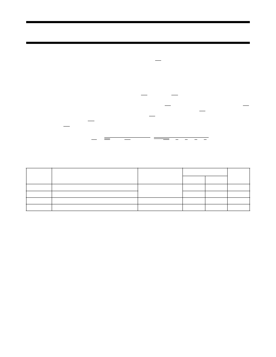
QUICK REFERENCE DATA
GND = 0 V; T
amb
= 25
∞
C; t
r
= t
f
= 6 ns
Notes
1. C
PD
is used to determine the dynamic power dissipation (P
D
in
µ
W):
P
D
= C
PD
◊
V
CC
2
◊
f
i
+
(C
L
◊
V
CC
2
◊
f
o
) where:
f
i
= input frequency in MHz
f
o
= output frequency in MHz
(C
L
◊
V
CC
2
◊
f
o
) = sum of outputs
C
L
= output load capacitance in pF
V
CC
= supply voltage in V
2. For HC the condition is V
I
= GND to V
CC
. For HCT the condition is V
I
= GND to V
CC
-
1.5 V
ORDERING INFORMATION
See
"74HC/HCT/HCU/HCMOS Logic Package Information"
.
SYMBOL
PARAMETER
CONDITIONS
TYPICAL
UNIT
HC
HCT
t
PHL
/ t
PLH
propagation delay CP to Q
n
C
L
= 15 pF; V
CC
= 5 V 21
23
ns
f
max
maximum clock frequency
57
58
MHz
C
I
input capacitance
3.5
3.5
pF
C
PD
power dissipation capacitance per package
notes 1 and 2
50
53
pF
TC = CE . {(UP/DN) . Q
0
. Q
3
+(UP/DN) . Q
0
. Q
1
. Q
2
. Q
3
}

December 1990
3
Philips Semiconductors
Product specification
BCD up/down counter
74HC/HCT4510
PIN DESCRIPTION
PIN NO.
SYMBOL
NAME AND FUNCTION
1
PL
parallel load input (active HIGH)
4, 12, 13, 3
D
0
to D
3
parallel inputs
5
CE
count enable input (active LOW)
6, 11, 14, 2
Q
0
to Q
3
parallel outputs
7
TC
terminal count output (active LOW)
8
GND
ground (0 V)
9
MR
asynchronous master reset input (active HIGH)
10
UP/DN
up/down control input
15
CP
clock input (LOW-to-HIGH, edge-triggered)
16
V
CC
positive supply voltage
Fig.1 Pin configuration.
Fig.2 Logic symbol.
Fig.3 IEC logic symbol.

December 1990
4
Philips Semiconductors
Product specification
BCD up/down counter
74HC/HCT4510
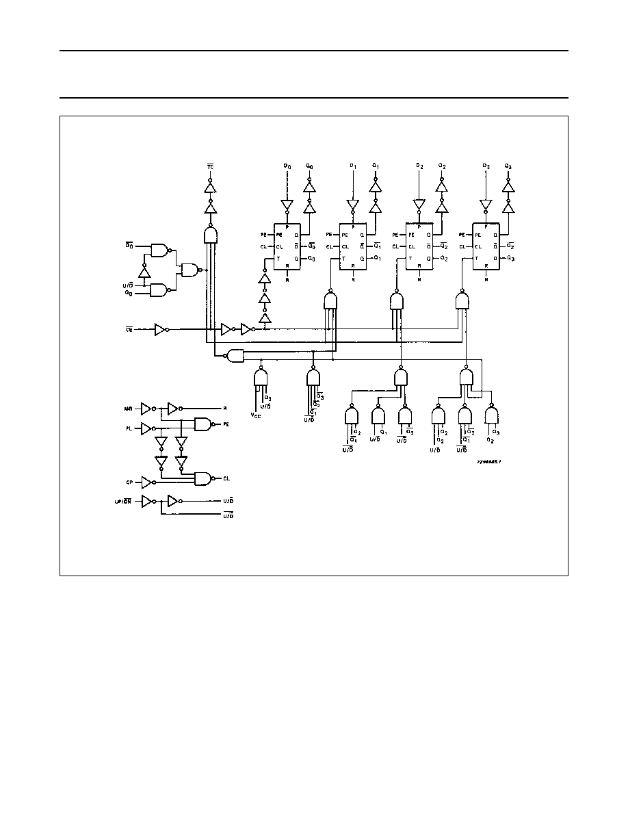
Fig.4 Functional diagram.
FUNCTION TABLE
Notes
1. H = HIGH voltage level
L = LOW voltage level
X = don't care
= LOW-to-HIGH clock transition
MR
PL
UP/DN
CE
CP
MODE
L
L
L
L
H
H
L
L
L
X
X
X
L
H
X
X
H
L
L
X
X
X
X
parallel load
no change
count down
count up
reset
Fig.5 Timing diagram.