2003 May 15
2
Philips Semiconductors
Product specification
PLL with band gap controlled VCO
74HCT9046A
FEATURES
·
Operation power supply voltage range from 4.5 to 5.5 V
·
Low power consumption
·
Inhibit control for ON/OFF keying and for low standby
power consumption
·
Centre frequency up to 17 MHz (typical) at V
CC
= 5.5 V
·
Choice of two phase comparators:
PC1: EXCLUSIVE-OR
PC2: Edge-triggered JK flip-flop.
·
No dead zone of PC2
·
Charge pump output on PC2, whose current is set by an
external resistor R
b
·
Centre frequency tolerance
±
10%
·
Excellent Voltage Controlled Oscillator (VCO) linearity
·
Low frequency drift with supply voltage and temperature
variations
·
On-chip band gap reference
·
Glitch free operation of VCO, even at very low
frequencies
·
Zero voltage offset due to op-amp buffering
·
ESD protection:
HBM EIA/JESD22-A114-A exceeds 2000 V
MM EIA/JESD22-A115-A exceeds 200 V.
APPLICATIONS
·
FM modulation and demodulation where a small centre
frequency tolerance is essential
·
Frequency synthesis and multiplication where a low jitter
is required (e.g. video picture-in-picture)
·
Frequency discrimination
·
Tone decoding
·
Data synchronization and conditioning
·
Voltage-to-frequency conversion
·
Motor-speed control.
GENERAL DESCRIPTION
The 74HCT9046A is a high-speed Si-gate CMOS device.
It is specified in compliance with "JEDEC standard no 7A".
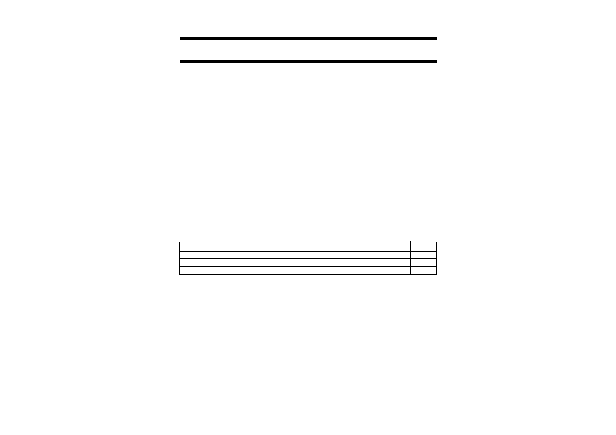
QUICK REFERENCE DATA
GND = 0 V; T
amb
= 25
°
C; t
r
= t
f
6 ns.
Notes
1. C
PD
is used to determine the dynamic power dissipation (P
D
in
µ
W).
P
D
= C
PD
×
V
CC
2
×
f
i
×
N +
(C
L
×
V
CC
2
×
f
o
) where:
f
i
= input frequency in MHz;
f
o
= output frequency in MHz;
C
L
= output load capacitance in pF;
V
CC
= supply voltage in Volts;
N = total load switching outputs;
(C
L
×
V
CC
2
×
f
o
) = sum of the outputs.
2. Applies to the phase comparator section only (pin INH = HIGH). For power dissipation of the VCO and demodulator
sections see Figs 26 to 28.
SYMBOL
PARAMETER
CONDITIONS
TYPICAL
UNIT
f
c
VCO centre frequency
C1 = 40 pF; R1 = 3 k
; V
CC
= 5 V 16
MHz
C
I
input capacitance
3.5
pF
C
PD
power dissipation capacitance per package
notes 1 and 2
20
pF
2003 May 15
3
Philips Semiconductors
Product specification
PLL with band gap controlled VCO
74HCT9046A
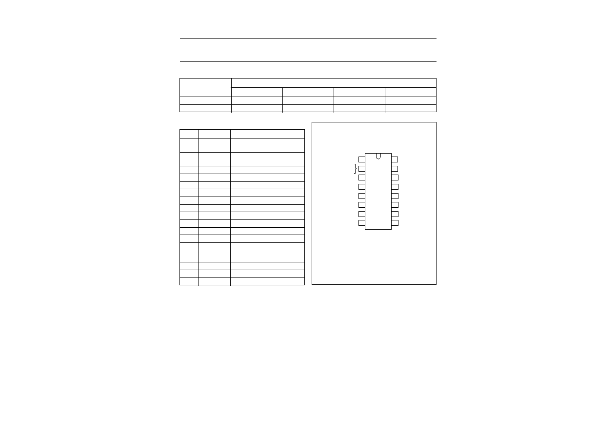
ORDERING INFORMATION
TYPE NUMBER
PACKAGE
PINS
PACKAGE
MATERIAL
CODE
74HCT9046AN
16
DIL16
plastic
SOT38Z
74HCT9046AD
16
SO16
plastic
SOT109A
PINNING
PIN
SYMBOL
DESCRIPTION
1
GND
ground (0 V) of phase
comparators
2
PC1_OUT/
PCP_OUT
phase comparator 1 output or
phase comparator pulse output
3
COMP_IN
comparator input
4
VCO_OUT
VCO output
5
INH
inhibit input
6
C1A
capacitor C1 connection A
7
C1B
capacitor C1 connection B
8
GND
ground (0 V) VCO
9
VCO_IN
VCO input
10
DEM_OUT
demodulator output
11
R1
resistor R1 connection
12
R2
resistor R2 connection
13
PC2_OUT
phase comparator 2 output;
current source adjustable with
R
b
14
SIG_IN
signal input
15
RB
bias resistor (R
b
) connection
16
V
CC
supply voltage
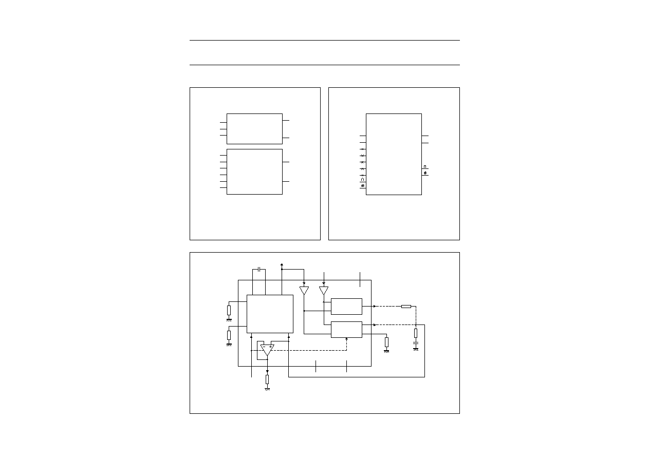
Fig.1 Pin configuration.
1
2
3
4
5
6
7
8
16
15
14
13
12
11
10
9
GND
PC1_OUT/
PCP_OUT
COMP_IN
VCO_OUT
C1B
C1A
GND
VCO_IN
DEM_OUT
R2
R1
PC2_OUT
SIG_IN
VCC
RB
9046A
MBD037
INH
2003
May
15
5
Philips Semiconductors
Product specification
PLL with band gap controlled VCO
74HCT9046A
This text is here in white to force landscape pages to be rotated correctly when browsing through the pdf in the Acrobat reader.This text is here in
_
white to force landscape pages to be rotated correctly when browsing through the pdf in the Acrobat reader.This text is here inThis text is here in
white to force landscape pages to be rotated correctly when browsing through the pdf in the Acrobat reader. white to force landscape pages to be ...
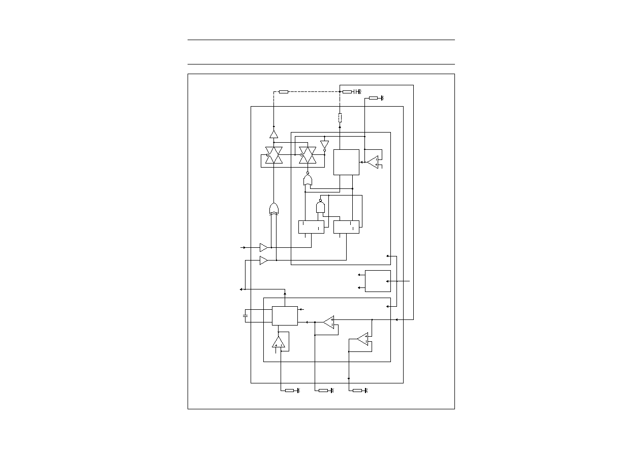
h
andbook, full pagewidth
MBD102
PCP
D
Q
CP
Q
R D
logic
1
D
Q
CP
Q
R D
logic
1
down
up
CHARGE
PUMP
Vref2
Vref2
Vref2
Vref1
Vref1
PC1_OUT/
PCP_OUT
PC2_OUT
b
Rb
RB
C2
R4
2
13
R3
15
COMP_IN
SIG_IN
3
14
PC1
BAND
GAP
5
INH
9
VCO
DEM_OUT
VCO_OUT
C1B
C1A
7
6
4
C1
12
R2
11
R1
10
R
fout
fin
R2
R1
s
VCO_IN
R3' = R /17
R3'
(1)
(1)
Fig.5 Logic diagram.