 | –≠–ª–µ–∫—Ç—Ä–æ–Ω–Ω—ã–π –∫–æ–º–ø–æ–Ω–µ–Ω—Ç: 74HCT9115 | –°–∫–∞—á–∞—Ç—å:  PDF PDF  ZIP ZIP |

DATA SHEET
Product specification
Supersedes data of March 1988
File under Integrated Circuits, IC06
December 1990
INTEGRATED CIRCUITS
74HC/HCT9115
Nine wide Schmitt trigger buffer;
open drain outputs
For a complete data sheet, please also download:
∑
The IC06 74HC/HCT/HCU/HCMOS Logic Family Specifications
∑
The IC06 74HC/HCT/HCU/HCMOS Logic Package Information
∑
The IC06 74HC/HCT/HCU/HCMOS Logic Package Outlines

December 1990
2
Philips Semiconductors
Product specification
Nine wide Schmitt trigger buffer;
open drain outputs
74HC/HCT9115
FEATURES
∑
Schmitt trigger action on all data inputs
∑
Output capability: standard (open drain)
∑
I
CC
category: MSI
GENERAL DESCRIPTION
The 74HC/HCT9115 are high-speed Si-gate CMOS
devices and are pin compatible with low power Schottky
TTL (LSTTL). They are specified in compliance with
JEDEC standard no. 7A.
The 74HC/HCT9115 are nine wide Schmitt trigger buffer
with open drain outputs and Schmitt trigger inputs.
The Schmitt trigger action in the data inputs transform
slowly changing input signals into sharply defined
jitter-free output signals.
The 74HC/HCT9115 have open-drain N-transistor
outputs, which are not clamped by a diode connected to
V
CC
. In the OFF-state, i.e. when one input is HIGH, the
output may be pulled to any voltage between GND and
V
Omax
. This allows the device to be used as a
LOW-to-HIGH or HIGH-to-LOW level shifter. For digital
operation and OR-tied output applications, these devices
must have a pull-up resistor to establish a logic HIGH level.
The "9115" is identical to the "9114" but has non-inverting
outputs.
QUICK REFERENCE DATA
GND = 0 V; T
amb
= 25
∞
C; t
r
= t
f
= 6 ns
Notes
1. C
PD
is used to determine the dynamic power dissipation (P
D
in
µ
W):
P
D
= C
PD
◊
V
CC
2
◊
f
i
+
(C
L
◊
V
CC
2
◊
f
o
) where:
f
i
= input frequency in MHz
f
o
= output frequency in MHz
(C
L
◊
V
CC
2
◊
f
o
) = sum of outputs
C
L
= output load capacitance in pF
V
CC
= supply voltage in V
2. For HC the condition is V
I
= GND to V
CC
For HCT the condition is V
I
= GND to V
CC
-
1.5 V
ORDERING INFORMATION
See
"74HC/HCT/HCU/HCMOS Logic Package Information"
.
SYMBOL
PARAMETER
CONDITIONS
TYPICAL
UNIT
HC
HCT
t
PHL
/ t
PLZ
propagation delay A
n
to Y
n
C
L
= 15 pF; V
CC
= 5 V
12
13
ns
C
I
input capacitance
3.5
3.5
pF
C
PD
power dissipation capacitance per buffer
notes 1 and 2
5
5
pF
December 1990
3
Philips Semiconductors
Product specification
Nine wide Schmitt trigger buffer;
open drain outputs
74HC/HCT9115
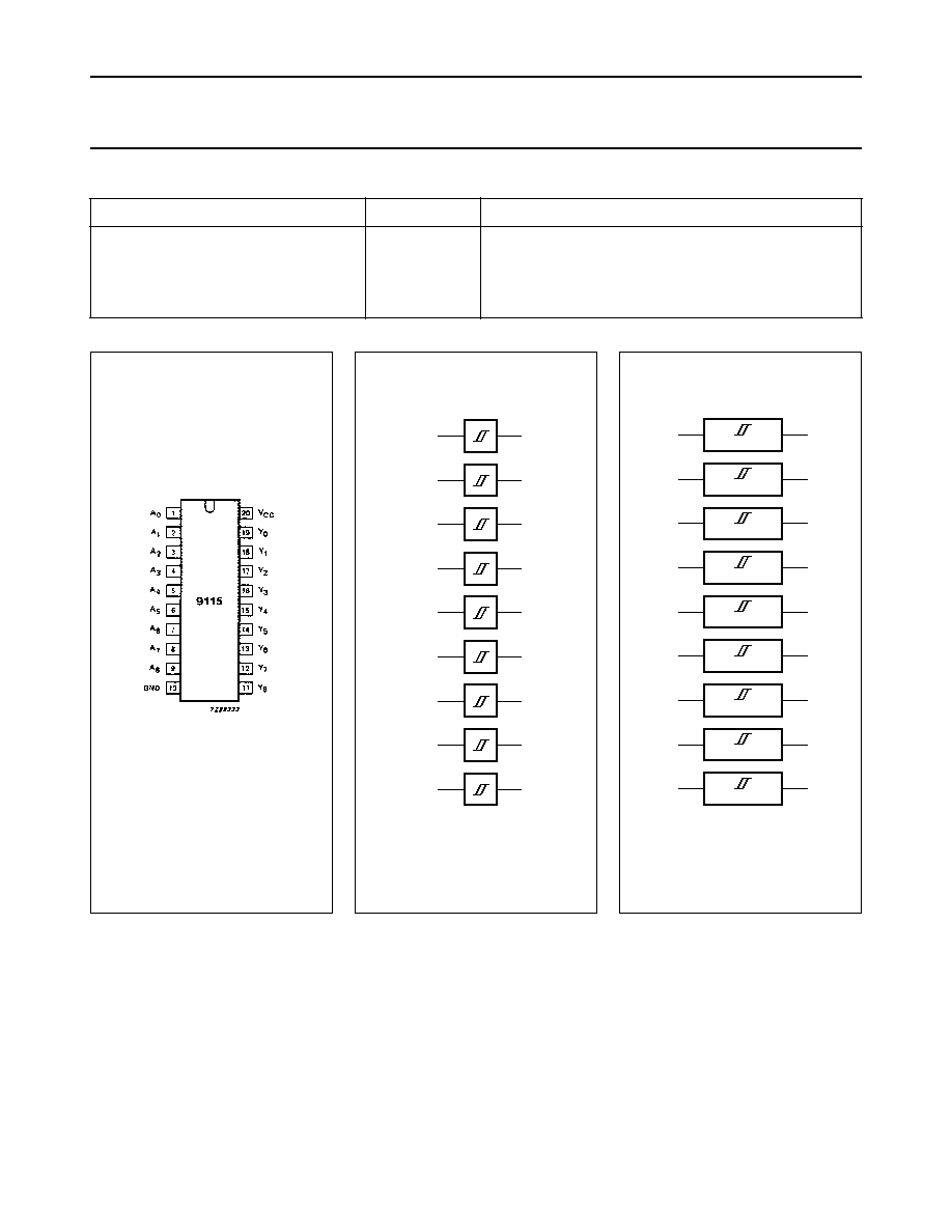
PIN DESCRIPTION
PIN NO.
SYMBOL
NAME AND FUNCTION
1, 2, 3, 4, 5, 6, 7, 8, 9
A
0
to A
8
data inputs
10
GND
ground (0 V)
19, 18, 17, 16, 15, 14, 13, 12, 11
Y
0
to Y
8
data outputs
20
V
CC
positive supply voltage
Fig.1 Pin configuration.
Fig.2 Logic diagram.
alfpage
MBA016
1
2
3
4
5
6
7
8
9
A 8
A 0
A 3
A 1
A 5
A 4
A 2
A 6
A 7
Y 8
Y 0
Y 3
Y 1
Y 5
Y 4
Y 2
Y 6
Y 7
19
18
12
14
15
11
13
16
17
Fig.3 IEC logic diagram.
fpage
3
4
5
6
7
8
9
11
12
13
14
15
16
17
1
2
18
19
MBA013

December 1990
4
Philips Semiconductors
Product specification
Nine wide Schmitt trigger buffer;
open drain outputs
74HC/HCT9115
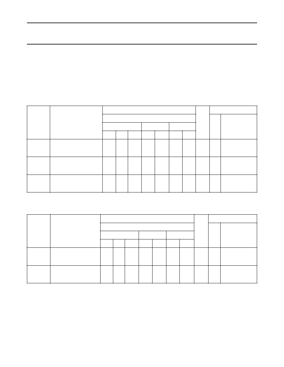
FUNCTION TABLE
Notes
1. H = HIGH voltage level
L = LOW voltage level
Z = high impedance OFF-state
INPUTS
OUTPUTS
A
n
Y
n
L
H
L
Z
Fig.4 Functional diagram.
Fig.5 Logic diagram (one Schmitt trigger).
handbook, halfpage
MBA022
An
GND
Yn
December 1990
5
Philips Semiconductors
Product specification
Nine wide Schmitt trigger buffer;
open drain outputs
74HC/HCT9115
DC CHARACTERISTICS FOR 74HC
For the DC characteristics see
"74HC/HCT/HCU/HCMOS Logic Family Specifications"
.
Transfer characteristics are given below.
Output capability: standard
I
CC
category: MSI
TRANSFER CHARACTERISTICS FOR 74HC
Voltages are referred to GND (ground = 0 V)
AC CHARACTERISTICS FOR 74HC
GND = 0 V; t
r
= t
f
= 6 ns; C
L
= 50 pF
SYMBOL
PARAMETER
T
amb
(
∞
C)
UNIT
TEST CONDITIONS
74HC
V
CC
(V)
WAVEFORMS
+
25
-
40 to
+
85
-
40 to
+
125
min.
typ.
max. min.
max.
min.
max.
V
T
+
positive-going threshold
0.70
1.75
2.30
1.13
2.37
3.11
1.50
3.15
4.20
0.70
1.75
2.30
1.50
3.15
4.20
0.70
1.75
2.30
1.50
3.15
4.20
V
2.0
4.5
6.0
Fig.6
V
T
-
negative-going threshold
0.30
1.35
1.80
0.70
1.80
2.43
1.10
2.40
3.30
0.30
1.35
1.80
1.10
2.40
3.30
0.30
1.35
1.80
1.10
2.40
3.30
V
2.0
4.5
6.0
Fig.6
V
H
hysteresis (V
T
+
-
V
T
-
)
0.2
0.4
0.5
0.43
0.57
0.68
0.80
1.00
1.10
0.18
0.40
0.50
0.80
1.00
1.10
0.15
0.40
0.50
0.80
1.00
1.10
V
2.0
4.5
6.0
Fig.6
SYMBOL
PARAMETER
T
amb
(
∞
C)
UNIT
TEST CONDITIONS
74HC
V
CC
(V)
WAVEFORMS
+
25
-
40 to
+
85
-
40 to
+
125
min. typ.
max. min.
max. min.
max.
t
PHL
/ t
PLZ
propagation delay
A
n
to Y
n
36
13
10
115
22
19
140
28
24
165
33
28
ns
2.0
4.5
6.0
Fig.7
t
THL
output transition time
19
7
6
75
15
13
95
19
16
110
22
19
ns
2.0
4.5
6.0
Fig.7