Philips Semiconductors
Product specification
74LV154
4-to-16 line decoder/demultiplexer
2
1998 Apr 28
853≠1939 19309
FEATURES
∑
Optimized for low voltage applications: 1.0 to 3.6 V
∑
Accepts TTL input levels between V
CC
= 2.7 V and V
CC
= 3.6 V
∑
Typical V
OLP
(output ground bounce) < 0.8 V at V
CC
= 3.3 V,
T
amb
= 25
∞
C
∑
Typical V
OHV
(output V
OH
undershoot) > 2 V at V
CC
= 3.3 V,
T
amb
= 25
∞
C
∑
16-line demultiplexing capability
∑
Decodes 4 binary-coded inputs into one of 16 mutually
exclusive outputs
∑
2-input enable gate for strobing or expansion
∑
Output capability: standard
∑
I
CC
category: MSI
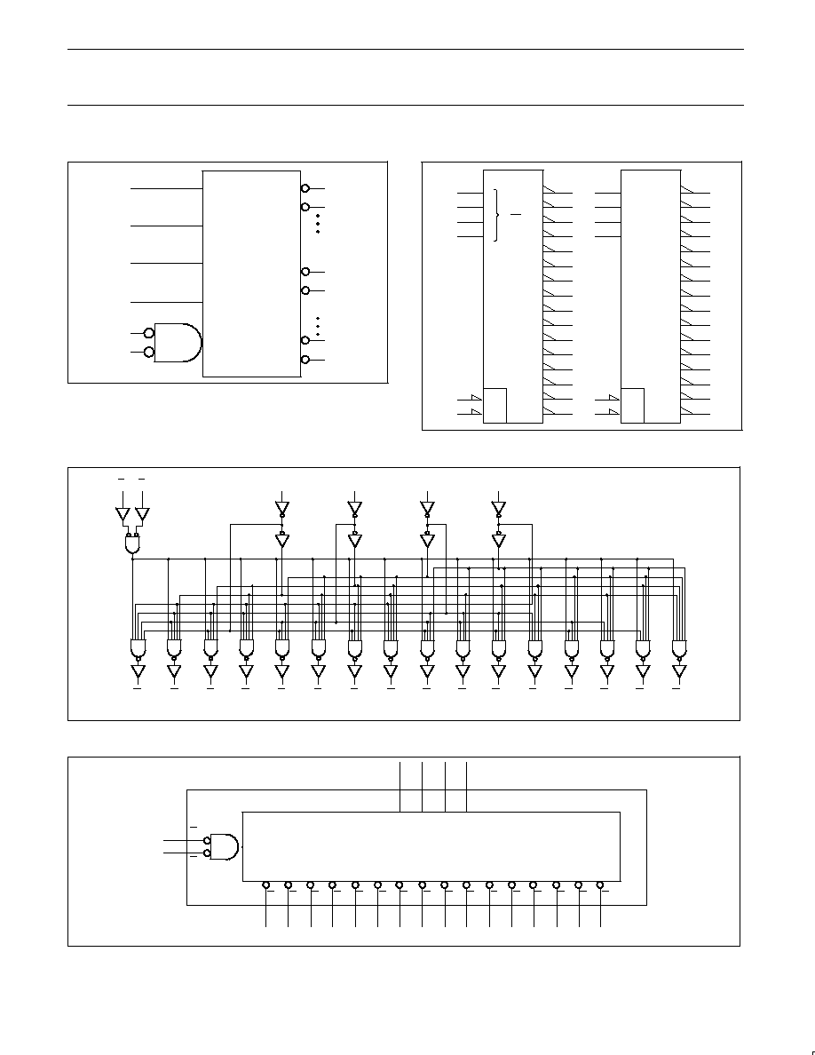
DESCRIPTION
The 74LV154 is a low-voltage CMOS device and is pin and function
compatible with 74HC/HCT154.
The 74LV154 decoders accept four active HIGH binary address
inputs (A
0
to A
3
) and provide 16 mutually exclusive active LOW
outputs(Y
0
to Y
15
).
The 2-input enable inputs (E
0
, E
1)
can be used to strobe the
decoder to eliminate the normal decoding "glitches" on the outputs,
or it can be used for expansion of the decoder.
The enable input has two AND'ed inputs which must be LOW to
enable the outputs.
The 74LV154 can be used as a 1-to-16 demultiplexer by using one
of the enable inputs as the multiplexed data input.
When the other enable is LOW, the addressed output will follow the
state of the applied data.
QUICK REFERENCE DATA
GND = 0 V; T
amb
= 25
∞
C; t
r
= t
f
2.5 ns
SYMBOL
PARAMETER
CONDITIONS
TYPICAL
UNIT
t
PHL
/t
PLH
Propagation delay
A
n
, E
n
to Y
n
C
L
= 15 pF;
V
CC
= 3.3 V
11
ns
C
I
Input capacitance
3.5
pF
C
PD
Power dissipation capacitance per gate
V
I
= GND to V
CC
1
60
pF
NOTE:
1. C
PD
is used to determine the dynamic power dissipation (P
D
in
µ
W)
P
D
= C
PD
◊
V
CC
2
◊
f
i
+
(C
L
◊
V
CC
2
◊
f
o
) where:
f
i
= input frequency in MHz; C
L
= output load capacitance in pF;
f
o
= output frequency in MHz; V
CC
= supply voltage in V;
(C
L
◊
V
CC
2
◊
f
o
) = sum of the outputs.
ORDERING INFORMATION
PACKAGES
TEMPERATURE RANGE
OUTSIDE NORTH AMERICA
NORTH AMERICA
PKG. DWG. #
24-Pin Plastic DIL
≠40
∞
C to +125
∞
C
74LV154 N
74LV154 N
SOT101-1
24-Pin Plastic SO
≠40
∞
C to +125
∞
C
74LV154 D
74LV154 D
SOT137-1
24-Pin Plastic SSOP Type II
≠40
∞
C to +125
∞
C
74LV154 DB
74LV154 DB
SOT340-1
24-Pin Plastic TSSOP Type I
≠40
∞
C to +125
∞
C
74LV154 PW
74LV154PW DH
SOT355-1
PIN CONFIGURATION
SV00544
1
2
3
4
5
6
7
8
9
10
11
12
Y 0
Y 1
Y 2
Y 3
Y 4
Y 5
Y 6
Y 7
Y 8
Y 9
Y 10
GND
V CC
A 0
A 1
A 2
A 3
E 1
E 0
Y 15
Y 14
Y 13
Y 12
Y 11
24
23
22
21
20
19
18
17
16
15
14
13
PIN DESCRIPTION
PIN NUMBER
SYMBOL
FUNCTION
1, 2, 3, 4, 5, 6, 7,
8, 9, 10, 11, 13,
14, 15, 16, 17
Y
0
to Y
15
Outputs (active LOW)
18, 19
E
0
, E
1
Enable inputs (active LOW)
12
GND
Ground (0 V)
23, 22, 21, 20
A
0
to A
3
Address inputs
16
V
CC
Positive supply voltage
Philips Semiconductors
Product specification
74LV154
4-to-16 line decoder/demultiplexer
1998 Apr 28
4
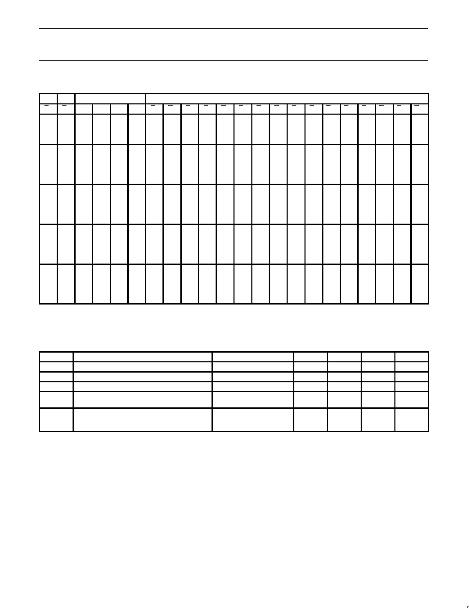
FUNCTION TABLE
INPUTS
OUTPUTS
E
0
E
1
A
0
A
1
A
2
A
3
Y
0
Y
1
Y
2
Y
3
Y
4
Y
5
Y
6
Y
7
Y
8
Y
9
Y
10
Y
11
Y
12
Y
13
Y
14
Y
15
H
H
X
X
X
X
H
H
H
H
H
H
H
H
H
H
H
H
H
H
H
H
H
L
X
X
X
X
H
H
H
H
H
H
H
H
H
H
H
H
H
H
H
H
L
H
X
X
X
X
H
H
H
H
H
H
H
H
H
H
H
H
H
H
H
H
L
L
L
L
L
L
L
H
H
H
H
H
H
H
H
H
H
H
H
H
H
H
L
L
H
L
L
L
H
L
H
H
H
H
H
H
H
H
H
H
H
H
H
H
L
L
L
H
L
L
H
H
L
H
H
H
H
H
H
H
H
H
H
H
H
H
L
L
H
H
L
L
H
H
H
L
H
H
H
H
H
H
H
H
H
H
H
H
L
L
L
L
H
L
H
H
H
H
L
H
H
H
H
H
H
H
H
H
H
H
L
L
H
L
H
L
H
H
H
H
H
L
H
H
H
H
H
H
H
H
H
H
L
L
L
H
H
L
H
H
H
H
H
H
L
H
H
H
H
H
H
H
H
H
L
L
H
H
H
L
H
H
H
H
H
H
H
L
H
H
H
H
H
H
H
H
L
L
L
L
L
H
H
H
H
H
H
H
H
H
L
H
H
H
H
H
H
H
L
L
H
L
L
H
H
H
H
H
H
H
H
H
H
L
H
H
H
H
H
H
L
L
L
H
L
H
H
H
H
H
H
H
H
H
H
H
L
H
H
H
H
H
L
L
H
H
L
H
H
H
H
H
H
H
H
H
H
H
H
L
H
H
H
H
L
L
L
L
H
H
H
H
H
H
H
H
H
H
H
H
H
H
L
H
H
H
L
L
H
L
H
H
H
H
H
H
H
H
H
H
H
H
H
H
H
L
H
H
L
L
L
H
H
H
H
H
H
H
H
H
H
H
H
H
H
H
H
H
L
H
L
L
H
H
H
H
H
H
H
H
H
H
H
H
H
H
H
H
H
H
H
L
NOTES:
H = HIGH voltage level
L
= LOW voltage level
X = don't care
RECOMMENDED OPERATING CONDITIONS
SYMBOL
PARAMETER
CONDITIONS
MIN
TYP
MAX
UNIT
V
CC
DC supply voltage
See Note 1
1.0
3.3
3.6
V
V
I
Input voltage
0
≠
V
CC
V
V
O
Output voltage
0
≠
V
CC
V
T
amb
Operating ambient temperature range in free air
See DC and AC
characteristics
≠40
≠40
+85
+125
∞
C
t
r
, t
f
Input rise and fall times
V
CC
= 1.0V to 2.0V
V
CC
= 2.0V to 2.7V
V
CC
= 2.7V to 3.6V
≠
≠
≠
≠
≠
≠
500
200
100
ns/V
NOTE:
1. The LV is guaranteed to function down to V
CC
= 1.0V (input levels GND or V
CC
); DC characteristics are guaranteed from V
CC
= 1.2V to V
CC
= 3.6V.
Philips Semiconductors
Product specification
74LV154
4-to-16 line decoder/demultiplexer
1998 Apr 28
5
ABSOLUTE MAXIMUM RATINGS
1, 2
In accordance with the Absolute Maximum Rating System (IEC 134).
Voltages are referenced to GND (ground = 0 V).
SYMBOL
PARAMETER
CONDITIONS
RATING
UNIT
V
CC
DC supply voltage
≠0.5 to +4.6
V
"
I
IK
DC input diode current
V
I
< ≠0.5 or V
I
> V
CC
+ 0.5V
20
mA
"
I
OK
DC output diode current
V
O
< ≠0.5 or V
O
> V
CC
+ 0.5V
50
mA
"
I
O
DC output source or sink current
≠ standard outputs
≠0.5V < V
O
< V
CC
+ 0.5V
25
mA
"
I
GND
,
"
I
CC
DC V
CC
or GND current for types with
≠ standard outputs
50
mA
T
stg
Storage temperature range
≠65 to +150
∞
C
P
TOT
Power dissipation per package
≠ plastic DIL
≠ plastic mini-pack (SO)
≠ plastic shrink mini-pack (SSOP and TSSOP)
for temperature range: ≠40 to +125
∞
C
above +70
∞
C derate linearly with 12 mW/K
above +70
∞
C derate linearly with 8 mW/K
above +60
∞
C derate linearly with 5.5 mW/K
750
500
400
mW
NOTES:
1. Stresses beyond those listed may cause permanent damage to the device. These are stress ratings only and functional operation of the
device at these or any other conditions beyond those indicated under "recommended operating conditions" is not implied. Exposure to
absolute-maximum-rated conditions for extended periods may affect device reliability.
2. The input and output voltage ratings may be exceeded if the input and output current ratings are observed.
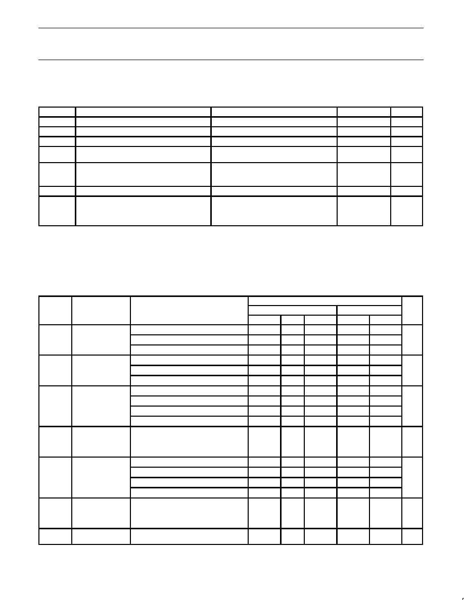
DC ELECTRICAL CHARACTERISTICS
Over recommended operating conditions. Voltages are referenced to GND (ground = 0 V).
LIMITS
SYMBOL
PARAMETER
TEST CONDITIONS
-40
∞
C to +85
∞
C
-40
∞
C to +125
∞
C
UNIT
MIN
TYP
1
MAX
MIN
MAX
HIGH l
l I
t
V
CC
= 1.2 V
0.9
0.9
V
IH
HIGH level Input
voltage
V
CC
= 2.0 V
1.4
1.4
V
voltage
V
CC
= 2.7 to 3.6 V
2.0
2.0
LOW l
l I
t
V
CC
= 1.2 V
0.3
0.3
V
IL
LOW level Input
voltage
V
CC
= 2.0 V
0.6
0.6
V
voltage
V
CC
= 2.7 to 3.6 V
0.8
0.8
V
CC
= 1.2 V; V
I
= V
IH
or V
IL;
≠I
O
= 100
µ
A
1.2
V
O
HIGH level output
V
CC
= 2.0 V; V
I
= V
IH
or V
IL;
≠I
O
= 100
µ
A
1.8
2.0
1.8
V
V
OH
voltage; all outputs
V
CC
= 2.7 V; V
I
= V
IH
or V
IL;
≠I
O
= 100
µ
A
2.5
2.7
2.5
V
V
CC
= 3.0 V; V
I
= V
IH
or V
IL;
≠I
O
= 100
µ
A
2.8
3.0
2.8
V
OH
HIGH level output
voltage;
STANDARD
outputs
V
CC
= 3.0 V; V
I
= V
IH
or V
IL;
≠I
O
= 6mA
2.40
2.82
2.20
V
V
CC
= 1.2 V; V
I
= V
IH
or V
IL;
I
O
= 100
µ
A
0
V
O
LOW level output
V
CC
= 2.0 V; V
I
= V
IH
or V
IL;
I
O
= 100
µ
A
0
0.2
0.2
V
V
OL
voltage; all outputs
V
CC
= 2.7 V; V
I
= V
IH
or V
IL;
I
O
= 100
µ
A
0
0.2
0.2
V
V
CC
= 3.0 V; V
I
= V
IH
or V
IL;
I
O
= 100
µ
A
0
0.2
0.2
V
OL
LOW level output
voltage;
STANDARD
outputs
V
CC
= 3.0 V; V
I
= V
IH
or V
IL;
I
O
= 6mA
0.25
0.40
0.50
V
I
I
Input leakage
current
V
CC
= 3.6 V; V
I
= V
CC
or GND
1.0
1.0
µ
A