
Philips
Semiconductors
74LV251
8-input multiplexer (3-State)
Product specification
Supersedes data of 1997 Apr 10
IC24 Data Handbook
1998 May 20
INTEGRATED CIRCUITS
Philips Semiconductors
Product specification
74LV251
8-input multiplexer (3-State)
2
1998 May 20
853≠1967 19420
FEATURES
∑
Optimized for low voltage applications: 1.0 to 3.6 V
∑
Accepts TTL input levels between V
CC
= 2.7 V and V
CC
= 3.6 V
∑
Typical V
OLP
(output ground bounce) < 0.8 V at V
CC
= 3.3 V,
T
amb
= 25
∞
C
∑
Typical V
OHV
(output V
OH
undershoot) > 2 V at V
CC
= 3.3 V,
T
amb
= 25
∞
C
∑
True and complement outputs
∑
Both outputs are 3-State for further multiplexer expansion
∑
Multifunction capability
∑
Permits multiplexing from n-lines to one line
∑
Output capability: standard
∑
I
CC
category: MSI
DESCRIPTION
The 74LV251 is a low-voltage Si-gate CMOS device and is pin and
function compatible with 74HC/HCT251.
The 74LV251 is an 8-input multiplexer with 8 binary inputs (I
0
to I
7
), an
output enable input (OE) and three select inputs (S
0
, S
1
, S
2
). One of
the eight binary inputs is selected by the select inputs and is routed to
the outputs (Y, Y). Both outputs are in the high impedance OFF-state
(Z) when the output enable input is HIGH, allowing multiplexer
expansion by tying the outputs.
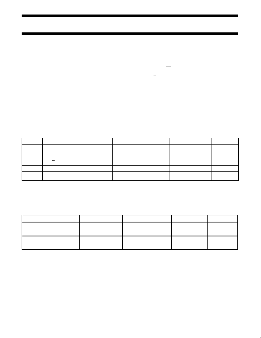
QUICK REFERENCE DATA
GND = 0 V; T
amb
= 25
∞
C; t
r
= t
f
2.5 ns
SYMBOL
PARAMETER
CONDITIONS
TYPICAL
UNIT
t
PHL
/t
PLH
Propagation delay
I
n
to Y
I
n
to Y
S
n
to Y
S
n
to Y
C
L
= 15 pF;
V
CC
= 3.3 V
14
16
19
20
ns
C
I
Input capacitance
3.5
pF
C
PD
Power dissipation capacitance per gate
V
CC
= 3.3 V
V
I
= GND to V
CC
1
44
pF
NOTE:
1. C
PD
is used to determine the dynamic power dissipation (P
D
in
µ
W)
P
D
= C
PD
◊
V
CC
2
◊
f
i
)
(C
L
◊
V
CC
2
◊
f
o
) where:
f
i
= input frequency in MHz; C
L
= output load capacitance in pF;
f
o
= output frequency in MHz; V
CC
= supply voltage in V;
(C
L
◊
V
CC
2
◊
f
o
) = sum of the outputs.
ORDERING INFORMATION
PACKAGES
TEMPERATURE RANGE
OUTSIDE NORTH AMERICA
NORTH AMERICA
PKG. DWG. #
16-Pin Plastic DIL
≠40
∞
C to +125
∞
C
74LV251 N
74LV251 N
SOT38-4
16-Pin Plastic SO
≠40
∞
C to +125
∞
C
74LV251 D
74LV251 D
SOT109-1
16-Pin Plastic SSOP Type II
≠40
∞
C to +125
∞
C
74LV251 DB
74LV251 DB
SOT338-1
16-Pin Plastic TSSOP Type I
≠40
∞
C to +125
∞
C
74LV251 PW
74LV251PW DH
SOT403-1

Philips Semiconductors
Product specification
74LV251
8-input multiplexer (3-State)
1998 May 20
3
PIN CONFIGURATION
SV00629
1
2
3
4
5
6
I
3
I
2
I
1
I
0
Y
Y
V
CC
I
4
I
5
16
15
14
13
12
11
7
8
GND
S
1
S
2
10
9
QE
I
6
I
7
S
0
PIN DESCRIPTION
PIN
NUMBER
SYMBOL
FUNCTION
4, 3, 2, 1, 15,
14, 13, 12
I
0
to I
7
Multiplexer inputs
5
Y
Multiplexer output
6
Y
Complementary multiplexer output
7
OE
3-State output enable input (active
LOW)
8
GND
Ground (0 V)
11, 10, 9
S
0
to S
2
Select inputs
16
V
CC
Positive supply voltage
LOGIC SYMBOL
SV00630
S0
S1
S2
OE
I1
I2
4
1
15
12
11
10
9
7
3
2
I5
I6
I7
I4
I3
I0
14
13
Y
Y
5
6
LOGIC SYMBOL (IEEE/IEC)
SV00631
1
2
2
4
11
7
1
15
12
3
10
2
9
5
6
7
4
3
0
0
EN
G
0
7
MUX
14
13
5
6
FUNCTIONAL DIAGRAM
SV00632
MULTIPLEXER
S 0
11
I 0
4
3
2
1
15
14
13
12
I 1
I 2
I3
I 4
I5
I 6
I7
S 1
10
S 2
OE
9
7
Y
6
Y
5
Philips Semiconductors
Product specification
74LV251
8-input multiplexer (3-State)
1998 May 20
4
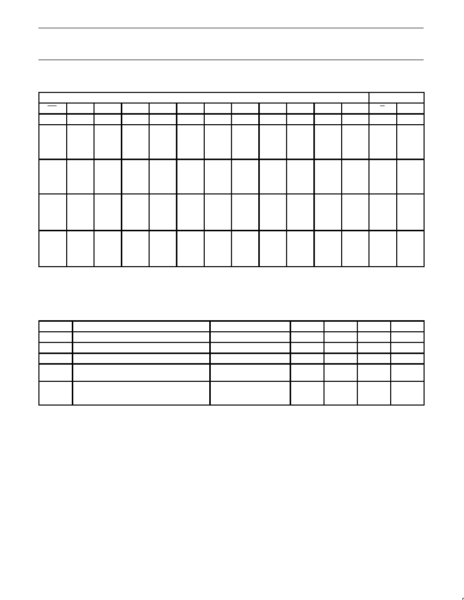
FUNCTION TABLE
INPUTS
OUTPUTS
OE
S
2
S
1
S
0
I
0
I
1
I
2
I
3
I
4
I
5
I
6
I
7
Y
Y
H
X
X
X
X
X
X
X
X
X
X
X
Z
Z
L
L
L
L
L
X
X
X
X
X
X
X
H
L
L
L
L
L
H
X
X
X
X
X
X
X
L
H
L
L
L
H
X
L
X
X
X
X
X
X
H
L
L
L
L
H
X
H
X
X
X
X
X
X
L
H
L
L
H
L
X
X
L
X
X
X
X
X
H
L
L
L
H
L
X
X
H
X
X
X
X
X
L
H
L
L
H
H
X
X
X
L
X
X
X
X
H
L
L
L
H
H
X
X
X
H
X
X
X
X
L
H
L
H
L
L
X
X
X
X
L
X
X
X
H
L
L
H
L
L
X
X
X
X
H
X
X
X
L
H
L
H
L
H
X
X
X
X
X
L
X
X
H
L
L
H
L
H
X
X
X
X
X
H
X
X
L
H
L
H
H
L
X
X
X
X
X
X
L
X
H
L
L
H
H
L
X
X
X
X
X
X
H
X
L
H
L
H
H
H
X
X
X
X
X
X
X
L
H
L
L
H
H
H
X
X
X
X
X
X
X
H
L
H
NOTES:
H =
HIGH voltage level
L
=
LOW voltage level
X =
don't care
Z =
high impedance OFF-state
RECOMMENDED OPERATING CONDITIONS
SYMBOL
PARAMETER
CONDITIONS
MIN
TYP
MAX
UNIT
V
CC
DC supply voltage
See Note 1
1.0
3.3
3.6
V
V
I
Input voltage
0
≠
V
CC
V
V
O
Output voltage
0
≠
V
CC
V
T
amb
Operating ambient temperature range in free air
See DC and AC
characteristics
≠40
≠40
+85
+125
∞
C
t
r
, t
f
Input rise and fall times
V
CC
= 1.0V to 2.0V
V
CC
= 2.0V to 2.7V
V
CC
= 2.7V to 3.6V
≠
≠
≠
≠
≠
≠
500
200
100
ns/V
NOTE:
1. The LV is guaranteed to function down to V
CC
= 1.0V (input levels GND or V
CC
); DC characteristics are guaranteed from V
CC
= 1.2V to V
CC
= 5.5V.

Philips Semiconductors
Product specification
74LV251
8-input multiplexer (3-State)
1998 May 20
5
ABSOLUTE MAXIMUM RATINGS
1, 2
In accordance with the Absolute Maximum Rating System (IEC 134).
Voltages are referenced to GND (ground = 0 V).
SYMBOL
PARAMETER
CONDITIONS
RATING
UNIT
V
CC
DC supply voltage
≠0.5 to +4.6
V
"
I
IK
DC input diode current
V
I
< ≠0.5 or V
I
> V
CC
+ 0.5V
20
mA
"
I
OK
DC output diode current
V
O
< ≠0.5 or V
O
> V
CC
+ 0.5V
50
mA
"
I
O
DC output source or sink current
≠ standard outputs
≠0.5V < V
O
< V
CC
+ 0.5V
25
mA
"
I
GND
,
"
I
CC
DC V
CC
or GND current for types with
≠ standard outputs
50
mA
T
stg
Storage temperature range
≠65 to +150
∞
C
P
TOT
Power dissipation per package
≠ plastic DIL
≠ plastic mini-pack (SO)
≠ plastic shrink mini-pack (SSOP and TSSOP)
for temperature range: ≠40 to +125
∞
C
above +70
∞
C derate linearly with 12 mW/K
above +70
∞
C derate linearly with 8 mW/K
above +60
∞
C derate linearly with 5.5 mW/K
750
500
400
mW
NOTES:
1. Stresses beyond those listed may cause permanent damage to the device. These are stress ratings only and functional operation of the
device at these or any other conditions beyond those indicated under "recommended operating conditions" is not implied. Exposure to
absolute-maximum-rated conditions for extended periods may affect device reliability.
2. The input and output voltage ratings may be exceeded if the input and output current ratings are observed.
DC ELECTRICAL CHARACTERISTICS
Over recommended operating conditions. Voltages are referenced to GND (ground = 0 V).
LIMITS
SYMBOL
PARAMETER
TEST CONDITIONS
-40
∞
C to +85
∞
C
-40
∞
C to +125
∞
C
UNIT
MIN
TYP
1
MAX
MIN
MAX
V
CC
= 1.2 V
0.9
0.9
V
IH
HIGH level Input
voltage
V
CC
= 2.0 V
1.4
1.4
V
voltage
V
CC
= 2.7 to 3.6 V
2.0
2.0
V
CC
= 1.2 V
0.3
0.3
V
IL
LOW level Input
voltage
V
CC
= 2.0 V
0.6
0.6
V
voltage
V
CC
= 2.7 to 3.6 V
0.8
0.8
V
CC
= 1.2 V; V
I
= V
IH
or V
IL;
≠I
O
= 100
µ
A
1.2
V
O
HIGH level output
V
CC
= 2.0 V; V
I
= V
IH
or V
IL;
≠I
O
= 100
µ
A
1.8
2.0
1.8
V
V
OH
voltage; all outputs
V
CC
= 2.7 V; V
I
= V
IH
or V
IL;
≠I
O
= 100
µ
A
2.5
2.7
2.5
V
V
CC
= 3.0 V; V
I
= V
IH
or V
IL;
≠I
O
= 100
µ
A
2.8
3.0
2.8
V
OH
HIGH level output
voltage;
STANDARD
outputs
V
CC
= 3.0 V; V
I
= V
IH
or V
IL;
≠I
O
= 6mA
2.40
2.82
2.20
V
V
CC
= 1.2 V; V
I
= V
IH
or V
IL;
I
O
= 100
µ
A
0
V
O
LOW level output
V
CC
= 2.0 V; V
I
= V
IH
or V
IL;
I
O
= 100
µ
A
0
0.2
0.2
V
V
OL
voltage; all outputs
V
CC
= 2.7 V; V
I
= V
IH
or V
IL;
I
O
= 100
µ
A
0
0.2
0.2
V
V
CC
= 3.0 V; V
I
= V
IH
or V
IL;
I
O
= 100
µ
A
0
0.2
0.2
V
OL
LOW level output
voltage;
STANDARD
outputs
V
CC
= 3.0 V; V
I
= V
IH
or V
IL;
I
O
= 6mA
0.25
0.40
0.50
V