 | ÐлекÑÑоннÑй компоненÑ: 74LV27D | СкаÑаÑÑ:  PDF PDF  ZIP ZIP |
Äîêóìåíòàöèÿ è îïèñàíèÿ www.docs.chipfind.ru
Philips
Semiconductors
74LV27
Triple 3-input NOR gate
Product specification
Supersedes data of 1997 Feb 03
IC24 Data Handbook
1998 Apr 20
INTEGRATED CIRCUITS
Philips Semiconductors
Product specification
74LV27
Triple 3-input NOR gate
2
1998 Apr 20
8531896 19258
FEATURES
·
Wide operating voltage: 1.0 to 5.5 V
·
Optimized for Low Voltage applications: 1.0 to 3.6 V
·
Accepts TTL input levels between V
CC
= 2.7 V and V
CC
= 3.6 V
·
Typical V
OLP
(output ground bounce) < 0.8 V at V
CC
= 3.3 V,
T
amb
= 25
°
C.
·
Typical V
OHV
(output V
OH
undershoot) > 2 V at V
CC
= 3.3 V,
T
amb
= 25
°
C.
·
Output capability: standard
·
I
CC
category: SSI
DESCRIPTION
The 74LV27 is a low-voltage Si-gate CMOS device and is pin and
function compatible with 74HC/HCT27.
The 74LV27 provides the 3-input NOR function.
QUICK REFERENCE DATA
GND = 0 V; T
amb
= 25
°
C; t
r
= t
f
2.5 ns
SYMBOL
PARAMETER
CONDITIONS
TYPICAL
UNIT
t
PHL
/t
PLH
Propagation delay
nA, nB, nC to nY
C
L
= 15 pF;
V
CC
= 3.3 V
8
ns
C
I
Input capacitance
3.5
pF
C
PD
Power dissipation capacitance per gate
See Notes 1 and 2
24
pF
NOTES:
1. C
PD
is used to determine the dynamic power dissipation (P
D
in
µ
W)
P
D
= C
PD
×
V
CC
2
×
f
i
)
(C
L
×
V
CC
2
×
f
o
) where:
f
i
= input frequency in MHz; C
L
= output load capacitance in pF;
f
o
= output frequency in MHz; V
CC
= supply voltage in V;
(C
L
×
V
CC
2
×
f
o
) = sum of the outputs.
2. The condition is V
I
= GND to V
CC.
ORDERING INFORMATION
PACKAGES
TEMPERATURE RANGE
OUTSIDE NORTH AMERICA
NORTH AMERICA
PKG. DWG. #
14-Pin Plastic DIL
40
°
C to +125
°
C
74LV27 N
74LV27 N
SOT27-1
14-Pin Plastic SO
40
°
C to +125
°
C
74LV27 D
74LV27 D
SOT108-1
14-Pin Plastic SSOP Type II
40
°
C to +125
°
C
74LV27 DB
74LV27 DB
SOT337-1
14-Pin Plastic TSSOP Type I
40
°
C to +125
°
C
74LV27 PW
74LV27PW DH
SOT402-1
PIN DESCRIPTION
PIN NUMBER
SYMBOL
NAME AND FUNCTION
1, 3, 9
1A 3A
Data inputs
2, 4, 10
1B 3B
Data inputs
13, 5, 11
1C 3C
Data inputs
7
GND
Ground (0 V)
12, 6, 8
1Y 3Y
Data outputs
14
V
CC
Positive supply voltage
FUNCTION TABLE
INPUTS
OUTPUTS
nA
nB
nC
nY
L
L
L
H
X
X
H
L
X
H
X
L
H
X
X
L
NOTES:
H = HIGH voltage level
L = LOW voltage level
X = don't care
Philips Semiconductors
Product specification
74LV27
Triple 3-input NOR gate
1998 Apr 20
3
PIN CONFIGURATION
1
2
3
4
5
6
7
1A
1B
2A
2B
2C
2Y
GND
V
CC
1C
1Y
3C
3B
3A
3Y
14
13
12
11
10
9
8
SV00446
LOGIC SYMBOL
2C
2A
2Y
5
3
6
2B
4
3C
3A
3Y
11
9
8
3B
10
1C
1A
1Y
13
1
12
1B
2
SV00447
LOGIC SYMBOL (IEEE/IEC)
2
4
10
1
3
9
13
5
11
12
6
8
SV00448
1
1
1
LOGIC DIAGRAM
A
C
Y
B
SV00449
RECOMMENDED OPERATING CONDITIONS
SYMBOL
PARAMETER
CONDITIONS
MIN
TYP
MAX
UNIT
V
CC
DC supply voltage
See Note 1
1.0
3.3
5.5
V
V
I
Input voltage
0
V
CC
V
V
O
Output voltage
0
V
CC
V
T
amb
Operating ambient temperature range in free air
See DC and AC
characteristics
40
40
+85
+125
°
C
t
r
, t
f
Input rise and fall times
V
CC
= 1.0V to 2.0V
V
CC
= 2.0V to 2.7V
V
CC
= 2.7V to 3.6V
V
CC
= 3.6V to 5.5V
500
200
100
50
ns/V
NOTE:
1. The LV is guaranteed to function down to V
CC
= 1.0V (input levels GND or V
CC
); DC characteristics are guaranteed from V
CC
= 1.2V to V
CC
= 5.5V.
Philips Semiconductors
Product specification
74LV27
Triple 3-input NOR gate
1998 Apr 20
4
ABSOLUTE MAXIMUM RATINGS
1, 2
In accordance with the Absolute Maximum Rating System (IEC 134).
Voltages are referenced to GND (ground = 0V).
SYMBOL
PARAMETER
CONDITIONS
RATING
UNIT
V
CC
DC supply voltage
0.5 to +7.0
V
"
I
IK
DC input diode current
V
I
< 0.5 or V
I
> V
CC
+ 0.5V
20
mA
"
I
OK
DC output diode current
V
O
< 0.5 or V
O
> V
CC
+ 0.5V
50
mA
"
I
O
DC output source or sink current
standard outputs
0.5V < V
O
< V
CC
+ 0.5V
25
mA
"
I
GND
,
"
I
CC
DC V
CC
or GND current for types with
standard outputs
50
mA
T
stg
Storage temperature range
65 to +150
°
C
P
TOT
Power dissipation per package
plastic DIL
plastic mini-pack (SO)
plastic shrink mini-pack (SSOP and TSSOP)
for temperature range: 40 to +125
°
C
above +70
°
C derate linearly with 12 mW/K
above +70
°
C derate linearly with 8 mW/K
above +60
°
C derate linearly with 5.5 mW/K
750
500
400
mW
NOTES:
1. Stresses beyond those listed may cause permanent damage to the device. These are stress ratings only and functional operation of the
device at these or any other conditions beyond those indicated under "recommended operating conditions" is not implied. Exposure to
absolute-maximum-rated conditions for extended periods may affect device reliability.
2. The input and output voltage ratings may be exceeded if the input and output current ratings are observed.
DC ELECTRICAL CHARACTERISTICS
Over recommended operating conditions. Voltages are referenced to GND (ground = 0V).
LIMITS
SYMBOL
PARAMETER
TEST CONDITIONS
-40
°
C to +85
°
C
-40
°
C to +125
°
C
UNIT
MIN
TYP
1
MAX
MIN
MAX
V
CC
= 1.2V
0.9
0.9
V
IH
HIGH level Input
V
CC
= 2.0V
1.4
1.4
V
V
IH
voltage
V
CC
= 2.7 to 3.6V
2.0
2.0
V
V
CC
= 4.5 to 5.5V
0.7
<
V
CC
0.7
<
V
CC
V
CC
= 1.2V
0.3
0.3
V
IL
LOW level Input
V
CC
= 2.0V
0.6
0.6
V
V
IL
voltage
V
CC
= 2.7 to 3.6V
0.8
0.8
V
V
CC
= 4.5 to 5.5
0.3
<
V
CC
0.3
<
V
CC
V
CC
= 1.2V; V
I
= V
IH
or V
IL;
I
O
= 100
µ
A
1.2
HIGH level output
V
CC
= 2.0V; V
I
= V
IH
or V
IL;
I
O
= 100
µ
A
1.8
2.0
1.8
V
OH
HIGH level output
voltage; all outputs
V
CC
= 2.7V; V
I
= V
IH
or V
IL;
I
O
= 100
µ
A
2.5
2.7
2.5
V
voltage all out uts
V
CC
= 3.0V; V
I
= V
IH
or V
IL;
I
O
= 100
µ
A
2.8
3.0
2.8
V
CC
= 4.5V; V
I
= V
IH
or V
IL;
I
O
= 100
µ
A
4.3
4.5
4.3
V
OH
HIGH level output
voltage;
V
CC
= 3.0V; V
I
= V
IH
or V
IL;
I
O
= 6mA
2.40
2.82
2.20
V
V
OH
g
STANDARD
outputs
V
CC
= 4.5V; V
I
= V
IH
or V
IL;
I
O
= 12mA
3.60
4.20
3.50
V
V
CC
= 1.2V; V
I
= V
IH
or V
IL;
I
O
= 100
µ
A
0
LOW level output
V
CC
= 2.0V; V
I
= V
IH
or V
IL;
I
O
= 100
µ
A
0
0.2
0.2
V
OL
LOW level output
voltage; all outputs
V
CC
= 2.7V; V
I
= V
IH
or V
IL;
I
O
= 100
µ
A
0
0.2
0.2
V
voltage all out uts
V
CC
= 3.0V; V
I
= V
IH
or V
IL;
I
O
= 100
µ
A
0
0.2
0.2
V
CC
= 4.5V; V
I
= V
IH
or V
IL;
I
O
= 100
µ
A
0
0.2
0.2
V
OL
LOW level output
voltage;
V
CC
= 3.0V; V
I
= V
IH
or V
IL;
I
O
= 6mA
0.25
0.40
0.50
V
V
OL
g
STANDARD
outputs
V
CC
= 4.5V; V
I
= V
IH
or V
IL;
I
O
= 12mA
0.35
0.55
0.65
V
I
I
Input leakage
current
V
CC
= 5.5V; V
I
= V
CC
or GND
1.0
1.0
µ
A
Philips Semiconductors
Product specification
74LV27
Triple 3-input NOR gate
1998 Apr 20
5
DC ELECTRICAL CHARACTERISTICS (Continued)
Over recommended operating conditions. Voltages are referenced to GND (ground = 0V).
LIMITS
SYMBOL
PARAMETER
TEST CONDITIONS
-40
°
C to +85
°
C
-40
°
C to +125
°
C
UNIT
MIN
TYP
1
MAX
MIN
MAX
I
CC
Quiescent supply
current; SSI
V
CC
= 5.5V; V
I
= V
CC
or GND; I
O
= 0
20.0
40
µ
A
I
CC
Additional
quiescent supply
current
V
CC
= 2.7V to 3.6V; V
I
= V
CC
0.6V
500
850
µ
A
NOTE:
1. All typical values are measured at T
amb
= 25
°
C.
AC CHARACTERISTICS
GND = 0V; t
r
= t
f
2.5ns; C
L
= 50pF; R
L
= 1K
CONDITION
LIMITS
SYMBOL
PARAMETER
WAVEFORM
CONDITION
40 to +85
°
C
40 to +125
°
C
UNIT
V
CC
(V)
MIN
TYP
1
MAX
MIN
MAX
1.2
50
Propagation delay
2.0
17
22
27
t
PHL/PLH
Propagation delay
nA, nB, nC to nY
Figures 1, 2
2.7
13
16
20
ns
nA, nB, nC to nY
3.0 to 3.6
10
2
13
16
4.5 to 5.5
11
14
NOTES:
1. Unless otherwise stated, all typical values are measured at T
amb
= 25
°
C
2. Typical values are measured at V
CC
= 3.3 V.
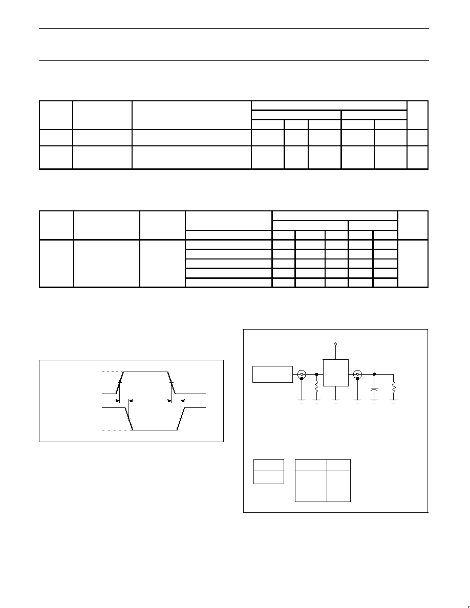
AC WAVEFORMS
V
M
= 1.5 V at V
CC
2.7 V and
3.6 V;
V
M
= 0.5
×
V
CC
at V
CC
<
2.7 V and
4.5 V;
V
OL
and V
OH
are the typical output voltage drop that occur with the
output load.
SV00420
VM
nA, nB, nC
INPUT
nY OUTPUT
VM
t PLH
t PHL
GND
VI
VOL
VOH
Figure 1. Input (nA, nB, nC) to output (nY) propagation delays.
TEST CIRCUIT
PULSE
GENERATOR
R
T
V
l
D.U.T.
V
O
C
L
R
L
= 1k
V
cc
Test Circuit for Outputs
DEFINITIONS
V
CC
V
I
< 2.7V
2.73.6V
V
CC
2.7V
TEST
t
PLH/
t
PHL
4.5 V
V
CC
R
L
= Load resistor
C
L
= Load capacitance includes jig and probe capacitiance
50pF
R
T
= Termination resistance should be equal to Z
OUT
of pulse generators.
SV00902
Figure 2. Load circuitry for switching times.
Document Outline
- FEATURES
- DESCRIPTION
- QUICK REFERENCE DATA
- ORDERING INFORMATION
- PIN DESCRIPTION
- FUNCTION TABLE
- PIN CONFIGURATION
- LOGIC SYMBOL (IEEE/IEC)
- LOGIC SYMBOL
- LOGIC DIAGRAM
- RECOMMENDED OPERATING CONDITIONS
- ABSOLUTE MAXIMUM RATINGS
- DC ELECTRICAL CHARACTERISTICS
- AC CHARACTERISTICS
- AC WAVEFORMS
- TEST CIRCUIT
- PACKAGE OUTLINES
- SOT27-1
- SOT108-1
- SOT337-1
- SOT402-1
- DEFINITIONS