 | –≠–ª–µ–∫—Ç—Ä–æ–Ω–Ω—ã–π –∫–æ–º–ø–æ–Ω–µ–Ω—Ç: 74LV4040D | –°–∫–∞—á–∞—Ç—å:  PDF PDF  ZIP ZIP |
Document Outline
- FEATURES
- DESCRIPTION
- QUICK REFERENCE DATA
- ORDERING INFORMATION
- PIN CONFIGURATION
- LOGIC SYMBOL
- PIN DESCRIPTION
- FUNCTIONAL DIAGRAM
- LOGIC SYMBOL (IEEE/IEC)
- LOGIC DIAGRAM
- FUNCTION TABLE
- ABSOLUTE MAXIMUM RATINGS
- RECOMMENDED OPERATING CONDITIONS
- DC CHARACTERISTICS FOR THE LV FAMILY
- AC CHARACTERISTICS
- AC WAVEFORMS
- TEST CIRCUIT
- PACKAGE OUTLINES
- SOT38-4
- SOT109-1
- SOT338-1
- SOT403-1
- Data sheet status
- Definitions
- Disclaimers

Philips
Semiconductors
74LV4040
12-stage binary ripple counter
Product specification
1998 Jun 23
INTEGRATED CIRCUITS
IC24 Data Handbook

Philips Semiconductors
Product specification
74LV4040
12-stage binary ripple counter
2
1998 Jun 23
853-2075 19619
FEATURES
∑
Optimized for Low Voltage applications: 1.0 to 5.5V
∑
Accepts TTL input levels between V
CC
= 2.7V and V
CC
= 3.6V
∑
Typical V
OLP
(output ground bounce)
t
0.8V @ V
CC
= 3.3V,
T
amb
= 25
∞
C
∑
Typical V
OHV
(output V
OH
undershoot)
u
2V @ V
CC
= 3.3V,
T
amb
= 25
∞
C
∑
Frequency dividing circuits
∑
Time delay circuits
∑
Control counters
∑
Output capability: standard
∑
I
CC
category: MSI
DESCRIPTION
The 74LV4040 is a low≠voltage Si≠gate CMOS device and is pin
and function compatible with 74HC/HCT4040.
The 74LV4040 is a 12-stage binary ripple counter with a click input
(CP), an overriding asynchronous master reset input (MR) and
twelve fully buffered parallel outputs (Q
0
to Q
11
). The counter is
advanced on the HIGH-to-LOW transition of CP. A HIGH on MR
clears all counter stages and forces all outputs LOW, independent of
the state of CP.
Each counter stage is a static toggle flip-flop.
QUICK REFERENCE DATA
GND = 0V; T
amb
= 25
∞
C; t
r
=t
f
v
2.5 ns
SYMBOL
PARAMETER
CONDITIONS
TYPICAL
UNIT
t
PHL
/t
PLH
Propagation delay
CP to Q
0
Q
n
to Q
n+1
MR to Q
n
C
L
= 15pF
V
CC
= 3.3V
12
7
16
ns
f
max
Maximum clock frequency
100
MHz
C
I
Input capacitance
3.5
pF
C
PD
Power dissipation capacitance per gate
Notes 1 and 2
30
pF
NOTES:
1. C
PD
is used to determine the dynamic power dissipation (P
D
in
µ
W)
P
D
= C
PD
V
CC
2
x f
i
)S
(C
L
V
CC
2
f
o
) where:
f
i
= input frequency in MHz; C
L
= output load capacity in pF;
f
o
= output frequency in MHz; V
CC
= supply voltage in V;
S
(C
L
V
CC
2
f
o
) = sum of the outputs.
2. The condition is V
I
= GND to V
CC
ORDERING INFORMATION
PACKAGES
TEMPERATURE RANGE
OUTSIDE NORTH AMERICA
NORTH AMERICA
PKG. DWG. #
16-Pin Plastic DIL
≠40
∞
C to +125
∞
C
74LV4040 N
74LV4040 N
SOT38-4
16-Pin Plastic SO
≠40
∞
C to +125
∞
C
74LV4040 D
74LV4040 D
SOT109-1
16-Pin Plastic SSOP Type II
≠40
∞
C to +125
∞
C
74LV4040 DB
74LV4040 DB
SOT338-1
16-Pin Plastic TSSOP Type I
≠40
∞
C to +125
∞
C
74LV4040 PW
74LV4040PW DH
SOT403-1
Philips Semiconductors
Product specification
74LV4040
12-stage binary ripple counter
1998 Jun 23
3
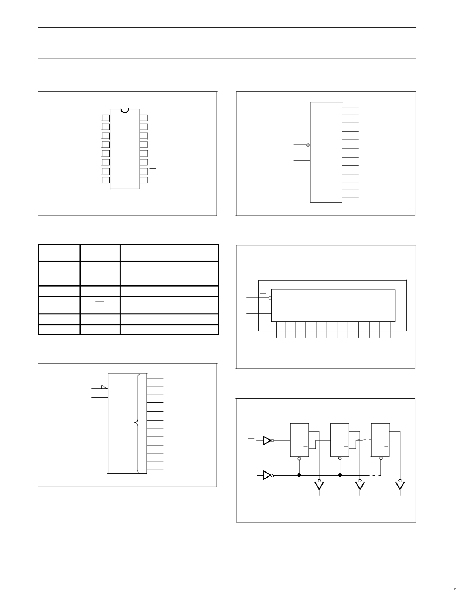
PIN CONFIGURATION
Q
11
Q
5
Q
4
Q
6
Q
3
Q
2
Q
1
GND
V
CC
Q
10
Q
9
Q
8
Q
7
MR
CP
Q
0
1
16
2
15
3
14
4
13
5
12
6
11
7
10
8
9
SV00316
Figure 1. Pin configuration
PIN DESCRIPTION
PIN
NUMBER
SYMBOL
FUNCTION
9, 7, 6, 5, 3,
2, 4, 13, 12,
14, 15, 1
Q
0
to Q
11
Parallel outputs
8
GND
Ground (0V)
10
CP
Clock input (HIGH-to-LOW, edge-
triggered)
11
MR
Master reset input (active HIGH)
16
V
CC
Positive supply voltage
LOGIC SYMBOL (IEEE/IEC)
+
CT=0
14
15
12
1
13
5
2
5
4
3
10
7
11
9
CTR12
0
11
CT
SV00318
Figure 2. IEC Logic symbol
LOGIC SYMBOL
Q
9
Q
10
Q
11
Q
3
Q
2
Q
4
Q
1
Q
8
Q
7
Q
6
Q
5
MR
CP
Q
0
14
15
12
1
13
5
2
6
4
3
11
7
10
9
SV00317
Figure 3. Logic symbol
FUNCTIONAL DIAGRAM
Q
9
Q
10
Q
11
Q
3
Q
2
Q
4
Q
1
Q
8
Q
7
Q
6
Q
5
MR
CP
Q
0
14
15
12
1
13
5
2
5
4
3
11
7
10
9
T
C
D
12-STAGE COUNTER
SV00319
Figure 4. Functional diagram
LOGIC DIAGRAM
T
Q
Q0
Q
Q
Q1
Q11
CP
MR
Q
Q
Q
T
T
R
D
R
D
R
D
FF0
FF3
FF11
SV00320
Figure 5. Logic diagram

Philips Semiconductors
Product specification
74LV4040
12-stage binary ripple counter
1998 Jun 23
4
CP INPUT
4.096
2.048
1.024
512
256
128
64
32
16
8
4
2
1
MR INPUT
Q
0
OUTPUT
Q
1
OUTPUT
Q
2
OUTPUT
Q
3
OUTPUT
Q
4
OUTPUT
Q
5
OUTPUT
Q
6
OUTPUT
SV00310
Q
7
OUTPUT
Q
8
OUTPUT
Q
9
OUTPUT
Q
10
OUTPUT
Q
11
OUTPUT
Figure 6. Timing diagram
FUNCTION TABLE
INPUTS
OUTPUTS
CP
MR
Q
0
, Q
3
to Q
13
∞
L
no change
±
L
count
X
H
L
NOTES:
H = HIGH voltage level
L = LOW voltage level
X = Don't care
∞
= LOW -to-HIGH clock transition
±
= HIGH-to-LOW clock transition

Philips Semiconductors
Product specification
74LV4040
12-stage binary ripple counter
1998 Jun 23
5
ABSOLUTE MAXIMUM RATINGS
1, 2
In accordance with the Absolute Maximum Rating System (IEC 134)
Voltages are referenced to GND (ground = 0V)
SYMBOL
PARAMETER
CONDITIONS
RATING
UNIT
V
CC
DC supply voltage
≠0.5 to +7.0
V
±
I
IK
DC input diode current
V
I
< ≠0.5 or V
I
> V
CC
+ 0.5V
20
mA
±
I
OK
DC output diode current
V
O
< ≠0.5 or V
O
> V
CC
+ 0.5V
50
mA
±
I
O
DC output source or sink current
≠ standard outputs
≠0.5V < V
O
< V
CC
+ 0.5V
25
mA
±
I
GND
,
±
I
CC
DC V
CC
or GND current for types with
≠standard outputs
50
mA
T
stg
Storage temperature range
≠65 to +150
∞
C
P
TOT
Power dissipation per package
≠plastic DIL
≠plastic mini-pack (SO)
≠plastic shrink mini-pack (SSOP and TSSOP)
for temperature range: ≠40 to +125
∞
C
above +70
∞
C derate linearly with 12mW/K
above +70
∞
C derate linearly with 8 mW/K
above +60
∞
C derate linearly with 5.5 mW/K
750
500
400
mW
NOTES:
1. Stresses beyond those listed may cause permanent damage to the device. These are stress ratings only and functional operation of the
device at these or any other conditions beyond those indicated under "recommended operating conditions" is not implied. Exposure to
absolute-maximum-rated conditions for extended periods may affect device reliability.
2. The input and output voltage ratings may be exceeded if the input and output current ratings are observed.
RECOMMENDED OPERATING CONDITIONS
SYMBOL
PARAMETER
CONDITIONS
MIN
TYP.
MAX
UNIT
V
CC
DC supply voltage
See Note
1
1.0
3.3
5.5
V
V
I
Input voltage
0
≠
V
CC
V
V
O
Output voltage
0
≠
V
CC
V
T
amb
Operating ambient temperature range in free
air
See DC and AC
characteristics
≠40
≠40
+85
+125
∞
C
t
r
, t
f
Input rise and fall times
V
CC
= 1.0V to 2.0V
V
CC
= 2.0V to 2.7V
V
CC
= 2.7V to 3.6V
V
CC
= 3.6V to 5.5V
≠
≠
≠
≠
≠
≠
≠
≠
500
200
100
50
ns/V
NOTE:
1. The LV is guaranteed to function down to V
CC
= 1.0V (input levels GND or V
CC
); DC characteristics are guaranteed from V
CC
= 1.2V to V
CC
= 5.5V.