Philips Semiconductors
Product specification
74LV4051
8-channel analog multiplexer/demultiplexer
2
1998 Jun 23
853-1998 19618
FEATURES
·
Optimized for low voltage applications: 1.0 to 6.0 V
·
Accepts TTL input levels between V
CC
= 2.7 V and V
CC
= 3.6 V
·
Low typ "ON" resistance:
60
W
at V
cc
V
EE
= 4.5 V
90
W
at V
cc
V
EE
= 3.0 V
145
W
at V
cc
V
EE
= 2.0 V
·
Logic level translation: to enable 3 V logic to communicate with
±
3
V analog signals
·
Typical "break before make" built in
·
Output capability: non-standard
·
I
CC
category: MSI
DESCRIPTION
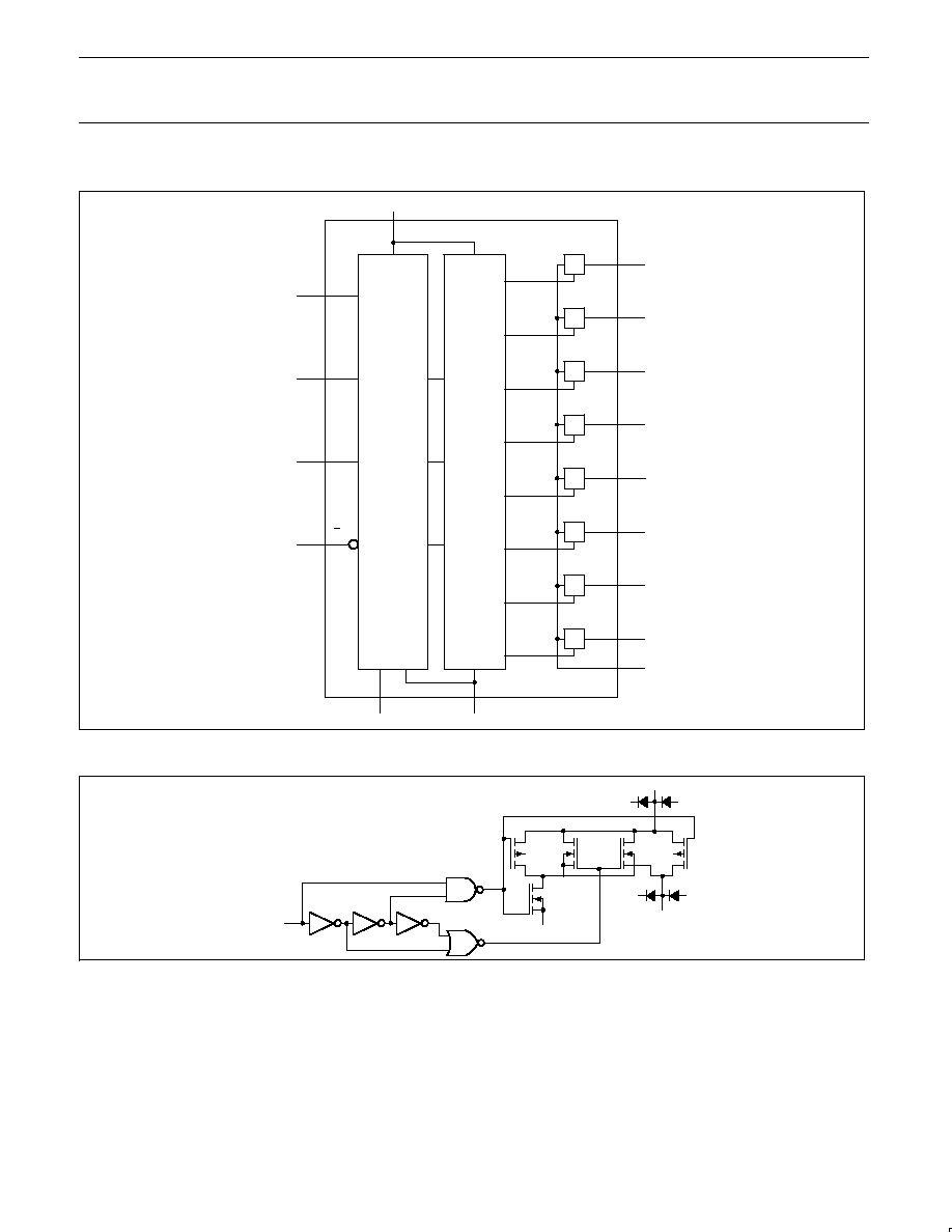
The 74LV4051 is a low-voltage CMOS device and is pin and
function compatible with the 74HC/HCT4051.
The 74LV4051 is an 8-channel analog multiplexer/demultiplexer with
three digital select inputs (S
0
to S
2
) an active LOW enable input (E),
eight independent inputs/outputs (Y
0
to Y
7
) and a common
input/output (Z).
With E LOW, one of the eight switches is selected (low impedance
ON-state) by S
0
to S
2.
With E HIGH, all switches are in the high
impedance OFF-state, independent of S
0
to S
2
.
V
CC
and GND are the supply voltage pins for the digital control
inputs (S
0
to S
2
, and E). The V
CC
to GND ranges are 1.0 to 6.0 V.
The analog inputs/outputs (Y
0
to Y
7
and Z) can swing between V
CC
as a positive limit and V
EE
as a negative limit. V
CC
- V
EE
may not
exceed 6.0 V. For operation as a digital multiplexer/demultiplexer,
V
EE
is connected to GND (typically ground).
QUICK REFERENCE DATA
GND = 0 V; T
amb
= 25
°
C; t
r
=t
f
2.5 ns
SYMBOL
PARAMETER
CONDITIONS
TYPICAL
UNIT
t
PZH
/t
PZL
Turn "ON" time
E to V
OS
S
n
to V
OS
C
L
= 15 pF
R
L
= 1K
W
V
CC
= 3.3 V
23
22
ns
t
PHZ
/t
PLZ
Turn "OFF" time
E to V
OS
S
n
to V
OS
25
20
ns
C
I
Input capacitance
3.5
C
PD
Power dissipation capacitance per switch
See Notes 1 and 2
25
pF
C
S
Maximum switch capacitance
independent (Y) common (Z)
5
25
F
NOTES:
1.
C
PD
is used to determine the dynamic power dissipation (P
D
in
µ
W)
P
D
= C
PD
×
V
CC
2
×
f
i
)
((C
L +
C
S
)
×
V
CC
2
×
f
o
) where:
f
i
= input frequency in MHz; C
L
= output load capacity in pF;
f
o
= output frequency in MHz; C
S
= maximum switch capacitance in pF;
V
CC
= supply voltage in V;
((C
L
+C
S
)
×
V
CC
2
×
f
o
) = sum of the outputs.
2.
The condition is V
I
= GND to V
CC
.
ORDERING INFORMATION
PACKAGES
TEMPERATURE RANGE
OUTSIDE NORTH AMERICA
NORTH AMERICA
Code
16-Pin Plastic DIL
40
°
C to +125
°
C
74LV4051 N
74LV4051 N
SOT38-4
16-Pin Plastic SO
40
°
C to +125
°
C
74LV4051 D
74LV4051 D
SOT109-1
16-Pin Plastic SSOP Type II
40
°
C to +125
°
C
74LV4051 DB
74LV4051 DB
SOT338-1
16-Pin Plastic TSSOP Type I
40
°
C to +125
°
C
74LV4051 PW
74LV4051PW DH
SOT403-1
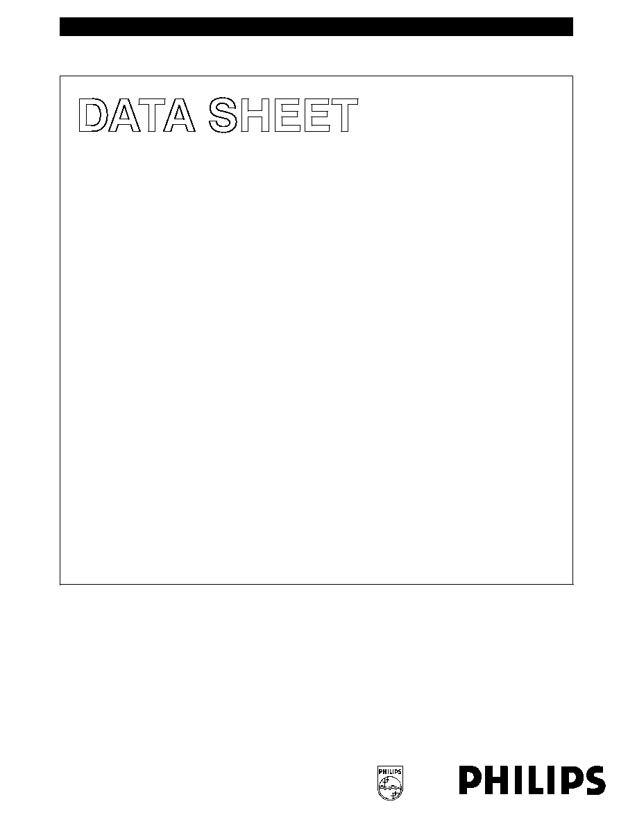
PIN CONFIGURATION
SV01702
14
13
12
11
10
9
8
7
6
5
4
3
2
1
15
16
GND
V
CC
Y
4
Y
6
Z
Y
7
Y
5
E
V
EE
Y
2
Y
1
Y
0
Y
3
S
0
S
1
S
2
PIN DESCRIPTION
PIN NUMBER
SYMBOL
FUNCTION
3
Z
Common input/output
6
E
Enable input (active LOW)
7
V
EE
Negative supply voltage
8
GND
Ground (0 V)
11, 10, 9
S
0
to S
2
Select inputs
13, 14, 15, 12,
1, 5, 2, 4
Y
0
to Y
7
Independent inputs/outputs
16
V
CC
Positive supply voltage
Philips Semiconductors
Product specification
74LV4051
8-channel analog multiplexer/demultiplexer
1998 Jun 23
5
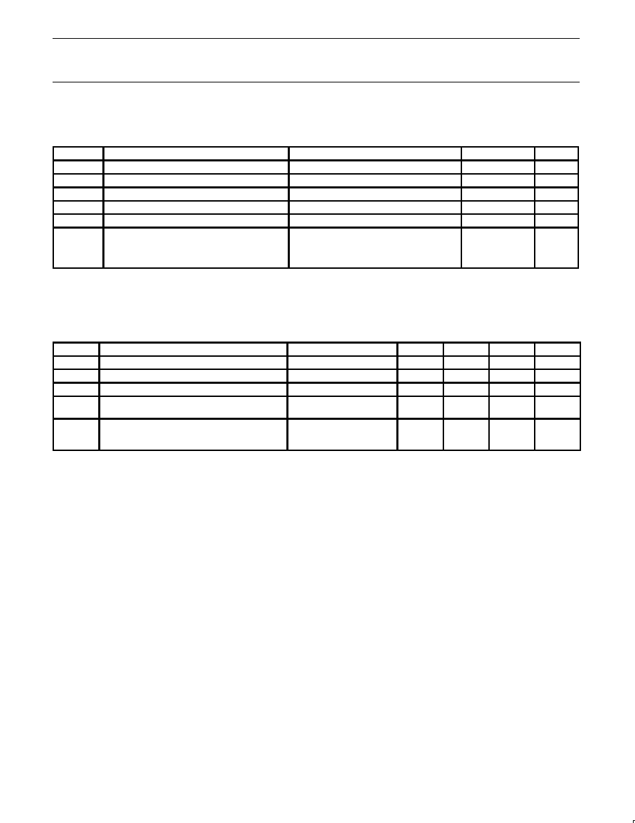
ABSOLUTE MAXIMUM RATINGS
1, 2
In accordance with the Absolute Maximum Rating System (IEC 134).
Voltages are referenced to GND (ground = 0 V).
SYMBOL
PARAMETER
CONDITIONS
RATING
UNIT
V
CC
DC supply voltage
0.5 to +7.0
V
"
I
IK
DC input diode current
V
I
< 0.5 or V
I
> V
CC
+ 0.5 V
20
mA
"
I
SK
DC switch diode current
V
S
< 0.5 or V
S
> V
CC
+ 0.5 V
20
mA
"
I
S
DC switch current
0.5 V < V
S
< V
CC
+ 0.5 V
25
mA
T
stg
Storage temperature range
65 to +150
°
C
P
TOT
Power dissipation per package
plastic DIL
plastic mini-pack (SO)
plastic shrink mini-pack (SSOP and TSSOP)
for temperature range: 40 to +125
°
C
above +70
°
C derate linearly with 12 mW/K
above +70
°
C derate linearly with 8 mW/K
above +60
°
C derate linearly with 5.5 mW/K
750
500
400
mW
NOTES:
1. Stresses beyond those listed may cause permanent damage to the device. These are stress ratings only and functional operation of the
device at these or any other conditions beyond those indicated under "recommended operating conditions" is not implied. Exposure to
absolute-maximum-rated conditions for extended periods may affect device reliability.
2. The input and output voltage ratings may be exceeded if the input and output current ratings are observed.
RECOMMENDED OPERATING CONDITIONS
SYMBOL
PARAMETER
CONDITIONS
MIN
TYP
MAX
UNIT
V
CC
DC supply voltage
See Note 1 and Figure 5
1.0
3.3
6.0
V
V
I
Input voltage
0
V
CC
V
V
O
Output voltage
0
V
CC
V
T
amb
Operating ambient temperature range in free air
See DC and AC
characteristics
40
40
+85
+125
°
C
t
r
, t
f
Input rise and fall times
V
CC
= 1.0 V to 2.0 V
V
CC
= 2.0 V to 2.7 V
V
CC
= 2.7 V to 6.0 V
500
200
100
ns/V
NOTE:
1. The LV is guaranteed to function down to V
CC
= 1.0V (input levels GND or V
CC
); DC characteristics are guaranteed from V
CC
= 1.2V to V
CC
= 6.0V.