Document Outline
- FEATURES
- DESCRIPTION
- QUICK REFERENCE DATA
- ORDERING INFORMATION
- PIN CONFIGURATION
- LOGIC SYMBOL
- PIN DESCRIPTION
- FUNCTION TABLE
- LOGIC SYMBOL (IEEE/IEC)
- RECOMMENDED OPERATING CONDITIONS
- ABSOLUTE MAXIMUM RATINGS
- DC ELECTRICAL CHARACTERISTICS
- AC CHARACTERISTICS
- AC WAVEFORMS
- TEST CIRCUIT
- PACKAGE OUTLINES
- SOT108-1
- SOT337-1
- SOT402-1
- DEFINITIONS
Philips
Semiconductors
74LVC125
Quad buffer/line driver; 3-State
Product specification
Supersedes data of February 1996
IC24 Data Handbook
1997 Mar 18
INTEGRATED CIRCUITS

Philips Semiconductors
Product specification
74LVC125
Quad buffer/line driver; 3-State
2
1997 Mar 18
853≠1951 17865
FEATURES
∑
Wide supply voltage range of 1.2 to 3.6 V
∑
In accordance with JEDEC standard no. 8-1A
∑
Inputs accept voltages up to 5.5 V
∑
CMOS lower power consumption
∑
Direct interface with TTL levels
∑
Output drive capability 50
W
transmission lines at 85
∞
C
DESCRIPTION
The 74LVC125 is a high performance, low-power, low-voltage
Si-gate CMOS device and superior to most advanced CMOS
compatible TTL families.
The 74LVC125 consists of four non-inverting buffers/line drivers with
3-State outputs. The 3-State outputs (nY) are controlled by the
output enable input (nOE). A HIGH at nOE causes the outputs to
assume a high impedance OFF-state.
QUICK REFERENCE DATA
GND = 0 V; T
amb
= 25
∞
C; t
r
= t
f
2.5 ns
SYMBOL
PARAMETER
CONDITIONS
TYPICAL
UNIT
t
PHL
/t
PLH
Propagation delay
nA to nY
C
L
= 15 pF;
V
CC
= 3.3 V
3.5
ns
C
I
Input capacitance
5.0
pF
C
PD
Power dissipation capacitance per buffer
Notes 1 and 2
22
pF
NOTES:
1. C
PD
is used to determine the dynamic power dissipation (P
D
in
µ
W)
P
D
= C
PD
◊
V
CC
2
◊
f
i
+
(C
L
◊
V
CC
2
◊
f
o
) where:
f
i
= input frequency in MHz; C
L
= output load capacity in pF;
f
o
= output frequency in MHz; V
CC
= supply voltage in V;
(C
L
◊
V
CC
2
◊
f
o
) = sum of the outputs.
2. The condition is V
I
= GND to V
CC
ORDERING INFORMATION
PACKAGES
TEMPERATURE RANGE
OUTSIDE NORTH AMERICA
NORTH AMERICA
PKG. DWG. #
14-Pin Plastic SO
≠40
∞
C to +85
∞
C
74LVC125 D
74LVC125 D
SOT108-1
14-Pin Plastic SSOP Type II
≠40
∞
C to +85
∞
C
74LVC125 DB
74LVC125 DB
SOT337-1
14-Pin Plastic TSSOP Type I
≠40
∞
C to +85
∞
C
74LVC125 PW
74LVC125PW DH
SOT402-1
PIN CONFIGURATION
SV00455
1
2
3
4
5
6
7
1OE
1A
1Y
2OE
2A
2Y
GND
V
CC
4OE
4A
4Y
3OE
3A
3Y
14
13
12
11
10
9
8
PIN DESCRIPTION
PIN
NUMBER
SYMBOL
NAME AND FUNCTION
1, 4, 10, 13
1OE ≠ 4OE
Data enable inputs (active LOW)
2, 5, 9, 12
1A ≠ 4A
Data inputs
3, 6, 8, 11
1Y ≠ 4Y
Data Outputs
7
GND
Ground (0 V)
14
V
CC
Positive supply voltage
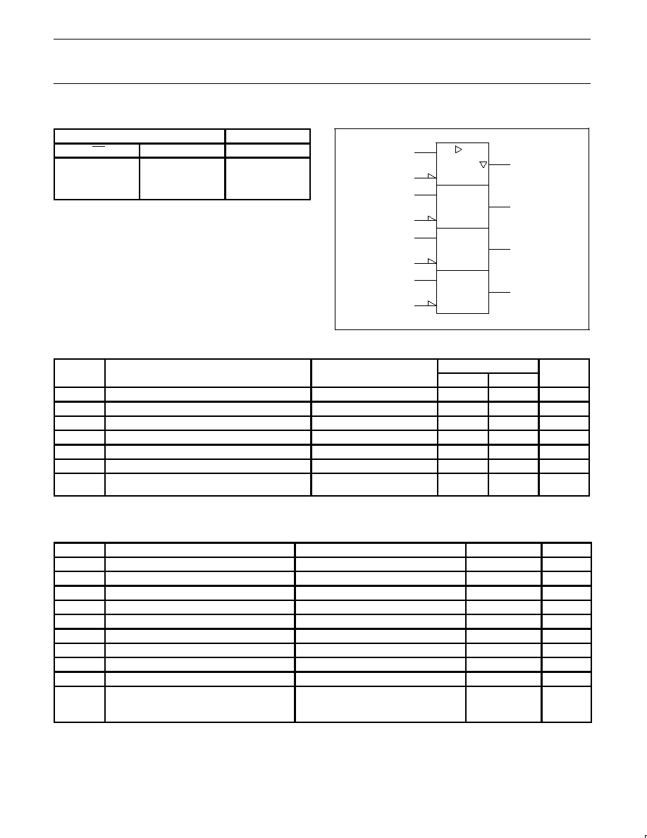
LOGIC SYMBOL
SV00456
1Y
2Y
3Y
4Y
1
2
3
1OE
1A
4
5
6
2OE
2A
10
9
8
3OE
3A
13
12
11
4OE
4A
Philips Semiconductors
Product specification
74LVC125
Quad buffer/line driver; 3-State
1997 Mar 18
3
FUNCTION TABLE
INPUTS
OUTPUT
nOE
nA
nY
L
L
L
L
H
H
H
X
Z
NOTES:
H = HIGH voltage level
L = LOW voltage level
X = don't care
Z = high impedance OFF-state
LOGIC SYMBOL (IEEE/IEC)
SV00457
1
2
EN1
1
3
4
5
6
10
9
8
13
12
11
RECOMMENDED OPERATING CONDITIONS
SYMBOL
PARAMETER
CONDITIONS
LIMITS
UNIT
SYMBOL
PARAMETER
CONDITIONS
MIN
MAX
UNIT
V
CC
DC supply voltage (for max. speed performance)
2.7
3.6
V
V
CC
DC supply voltage (for low-voltage applications)
1.2
3.6
V
V
I
DC input voltage range
0
5.5
V
V
I/O
DC input voltage range for I/Os
0
V
CC
V
V
O
DC output voltage range
0
V
CC
V
T
amb
Operating free-air temperature range
≠40
+85
∞
C
t
r
, t
f
Input rise and fall times
V
CC
= 1.2 to 2.7V
V
CC
= 2.7 to 3.6V
0
0
20
10
ns/V
ABSOLUTE MAXIMUM RATINGS
1
In accordance with the Absolute Maximum Rating System (IEC 134).
Voltages are referenced to GND (ground = 0 V).
SYMBOL
PARAMETER
CONDITIONS
RATING
UNIT
V
CC
DC supply voltage
≠0.5 to +6.5
V
I
IK
DC input diode current
V
I
t
0
≠50
mA
V
I
DC input voltage
Note 2
≠0.5 to +5.5
V
V
I/O
DC input voltage range for I/Os
≠0.5 to V
CC
+0.5
V
I
OK
DC output diode current
V
O
u
V
CC
or V
O
t
0
"
50
mA
V
OUT
DC output voltage
Note 2
≠0.5 to V
CC
+0.5
V
I
OUT
DC output source or sink current
V
O
= 0 to V
CC
"
50
mA
I
GND
, I
CC
DC V
CC
or GND current
"
100
mA
T
stg
Storage temperature range
≠60 to +150
∞
C
Power dissipation per package
P
TOT
≠ plastic mini-pack (SO)
above +70
∞
C derate linearly with 8 mW/K
500
mW
≠ plastic shrink mini-pack (SSOP and TSSOP)
above +60
∞
C derate linearly with 5.5 mW/K
500
mW
NOTES:
1. Stresses beyond those listed may cause permanent damage to the device. These are stress ratings only and functional operation of the
device at these or any other conditions beyond those indicated under "recommended operating conditions" is not implied. Exposure to
absolute-maximum-rated conditions for extended periods may affect device reliability.
2. The input and output voltage ratings may be exceeded if the input and output current ratings are observed.
Philips Semiconductors
Product specification
74LVC125
Quad buffer/line driver; 3-State
1997 Mar 18
4
DC ELECTRICAL CHARACTERISTICS
Over recommended operating conditions. Voltages are referenced to GND (ground = 0 V).
LIMITS
SYMBOL
PARAMETER
TEST CONDITIONS
Temp = -40
∞
C to +85
∞
C
UNIT
MIN
TYP
1
MAX
V
HIGH level Input voltage
V
CC
= 1.2V
V
CC
V
V
IH
HIGH level Input voltage
V
CC
= 2.7 to 3.6V
2.0
V
V
LOW level Input voltage
V
CC
= 1.2V
GND
V
V
IL
LOW level Input voltage
V
CC
= 2.7 to 3.6V
0.8
V
V
CC
= 2.7V; V
I
= V
IH
or V
IL
; I
O
= ≠12mA
V
CC
*
0.5
V
O
HIGH level output voltage
V
CC
= 3.0V; V
I
= V
IH
or V
IL
; I
O
= ≠100
µ
A
V
CC
*
0.2
V
CC
V
V
OH
HIGH level output voltage
V
CC
= 3.0V; V
I
= V
IH
or V
IL;
I
O
= ≠12mA
V
CC
*
0.6
V
V
CC
= 3.0V; V
I
= V
IH
or V
IL;
I
O
= ≠24mA
V
CC
*
1.0
V
CC
= 2.7V; V
I
= V
IH
or V
IL
; I
O
= 12mA
0.40
V
OL
LOW level output voltage
V
CC
= 3.0V; V
I
= V
IH
or V
IL
; I
O
= 100
µ
A
GND
0.20
V
V
CC
= 3.0V; V
I
= V
IH
or V
IL;
I
O
= 24mA
0.55
I
Input leakage current
V
= 3 6V; V = 5 5V or GND
Not for I/O pins
"
0 1
"
5
µ
A
I
I
Input leakage current
V
CC
= 3.6V; V
I
= 5.5V or GND
Not for I/O pins
"
0.1
"
5
µ
A
I
IHZ
/I
ILZ
Input current for common I/O pins
V
CC
= 3.6V; V
I
= V
CC
or GND
"
0.1
"
15
µ
A
I
OZ
3-State output OFF-state current
V
CC
= 3.6V; V
I
= V
IH
or V
IL
; V
O
= V
CC
or GND
0.1
"
10
µ
A
I
CC
Quiescent supply current
V
CC
= 3.6V; V
I
= V
CC
or GND; I
O
= 0
0.1
20
µ
A
I
CC
Additional quiescent supply current per
input pin
V
CC
= 2.7V to 3.6V; V
I
= V
CC
≠0.6V; I
O
= 0
5
500
µ
A
NOTE:
1. All typical values are at V
CC
= 3.3V and T
amb
= 25
∞
C.

Philips Semiconductors
Product specification
74LVC125
Quad buffer/line driver; 3-State
1997 Mar 18
5
AC CHARACTERISTICS
GND = 0 V; t
r
= t
f
= 2.5 ns; C
L
= 50 pF; R
L
= 500
W
; T
amb
= ≠40
_
C to +85
_
C.
LIMITS
SYMBOL
PARAMETER
WAVEFORM
V
CC
= 3.3V
±
0.3V
V
CC
= 2.7V
V
CC
= 1.2V
UNIT
MIN
TYP
1
MAX
MIN
TYP
MAX
TYP
t
PHL
t
PLH
Propagation delay
nA to nY
Figure 1, 3
3.5
6.5
3.9
7.0
ns
t
PZH
t
PZL
3-state output enable
time nOE to nY
Figure 2, 3
3.8
7.0
4.4
8.0
ns
t
PHZ
t
PLZ
3-state output disable
time nOE to nY
Figure 2, 3
3.3
5.5
4.0
6.5
ns
NOTE:
1. These typical values are at V
CC
= 3.3V and T
amb
= 25
∞
C.
AC WAVEFORMS
V
M
= 1.5 V at V
CC
w
2.7 V
V
M
= 0.5
◊
V
CC
at V
CC
< 2.7 V
V
OL
and V
OH
are the typical output voltage drop that occur with the
output load.
V
X
= V
OL
+ 0.3 V at V
CC
2.7 V;
V
X
= V
OL
+ 0.1
◊
V
CC
at V
CC
< 2.7 V;
V
Y
= V
OH
≠ 0.3 V at V
CC
2.7 V;
V
Y
= V
OH
≠ 0.1
◊
V
CC
at V
CC
< 2.7 V.
SV00459
VM
nA INPUT
nY OUTPUT
VM
tPLH
t PHL
GND
V
l
V OL
V OH
Figure 1. Input (nA) to output (nY) propagation delays.
SV00458
outputs
disabled
outputs
enabled
outputs
enabled
tPHZ
tPZH
tPZL
tPLZ
VX
VY
VM
VM
nOE Input
VI
GND
VCC
VOL
VOH
GND
OUTPUT
HIGH-to-OFF
OFF-to-HIGH
OUTPUT
LOW-to-OFF
OFF-to-LOW
VM
Figure 2. 3-State enable and disable times.
TEST CIRCUIT
PULSE
GENERATOR
V
I
R
T
D.U.T.
V
O
C
L
50pF
S
1
2
<
V
CC
Open
GND
500
500
V
CC
V
I
t
2.7V
V
CC
2.7V ≠ 3.6V
2.7V
Test
S
1
GND
t
PLZ
/t
PZL
2
<
V
CC
t
PHZ
/t
PZH
t
PLH
/t
PHL
Open
SY00003
V
CC
Figure 3. Load circuitry for switching times.